MAX3490EPA Просмотр технического описания (PDF) - Maxim Integrated
Номер в каталоге
Компоненты Описание
производитель
MAX3490EPA
Maxim Integrated

MAX3490EPA Datasheet PDF : 16 Pages
| |||
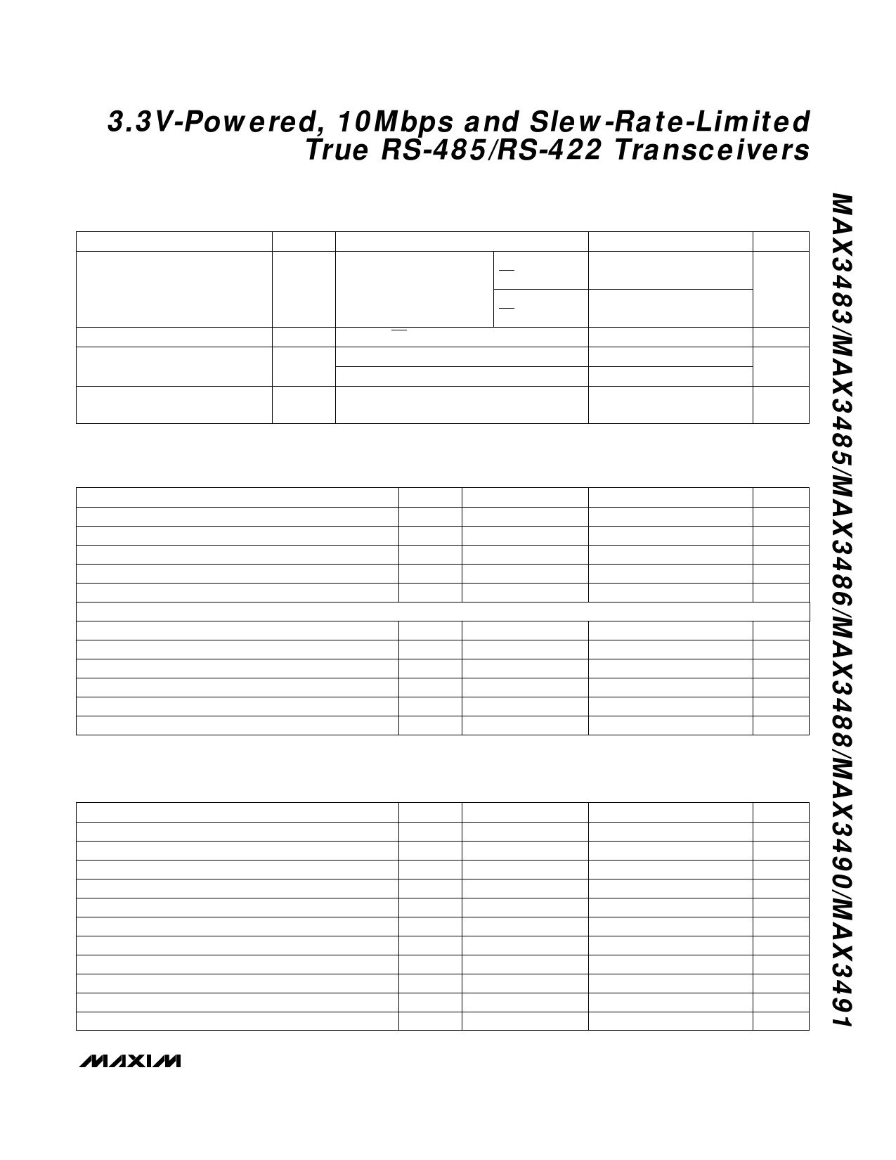
3.3V-Powered, 10Mbps and Slew-Rate-Limited
True RS-485/RS-422 Transceivers
DC ELECTRICAL CHARACTERISTICS (continued)
(VCC = 3.3V ±0.3V, TA = TMIN to TMAX, unless otherwise noted. Typical values are at TA = +25°C)
PARAMETER
SYMBOL
CONDITIONS
MIN
Supply Current
ICC
No load,
DI = 0V or VCC
DE = VCC,
RE = 0V or VCC
DE = 0V,
RE = 0V
Supply Current in Shutdown Mode
Driver Short-Circuit Output
Current
ISHDN
IOSD
DE = 0V, RE = VCC, DI = VCC or 0V
VOUT = -7V
VOUT = 12V
Receiver Short-Circuit Output
Current
IOSR 0V ≤ VRO ≤ VCC
±8
TYP MAX
1.1
2.2
0.95
0.002
1.9
1
-250
250
±60
UNITS
mA
µA
mA
mA
DRIVER SWITCHING CHARACTERISTICS—MAX3485, MAX3490, and MAX3491
(VCC = 3.3V, TA = +25°C)
PARAMETER
SYMBOL CONDITIONS
MIN TYP MAX
Driver Differential Output Delay
tDD RL = 60Ω, Figure 7
1
22
35
Driver Differential Output Transition Time
tTD RL = 60Ω, Figure 7
3
8
25
Driver Propagation Delay, Low-to-High Level
tPLH RL = 27Ω, Figure 8
7
22
35
Driver Propagation Delay, High-to-Low Level
tPHL RL = 27Ω, Figure 8
7
22
35
|tPLH - tPHL| Driver Propagation Delay Skew (Note 2)
tPDS RL = 27Ω, Figure 8
8
DRIVER OUTPUT ENABLE/DISABLE TIMES (MAX3485/MAX3491 only)
Driver Output Enable Time to Low Level
tPZL RL = 110Ω, Figure 10
45
90
Driver Output Enable Time to High Level
tPZH RL = 110Ω, Figure 9
45
90
Driver Output Disable Time from High Level
tPHZ RL = 110Ω, Figure 9
40
80
Driver Output Disable Time from Low Level
tPLZ RL = 110Ω, Figure 10
40
80
Driver Output Enable Time from Shutdown to Low Level
tPSL RL = 110Ω, Figure 10
650
900
Driver Output Enable Time from Shutdown to High Level tPSH RL = 110Ω, Figure 9
650
900
UNITS
ns
ns
ns
ns
ns
ns
ns
ns
ns
ns
ns
DRIVER SWITCHING CHARACTERISTICS—MAX3486
(VCC = 3.3V, TA = +25°C)
PARAMETER
SYMBOL CONDITIONS
MIN TYP MAX UNITS
Driver Differential Output Delay
tDD RL = 60Ω, Figure 7
24
48
70
ns
Driver Differential Output Transition Time
tTD RL = 60Ω, Figure 7
15
35
60
ns
Driver Propagation Delay, Low-to-High Level
tPLH RL = 27Ω, Figure 8
20
48
70
ns
Driver Propagation Delay, High-to-Low Level
tPHL RL = 27Ω, Figure 8
20
48
70
ns
|tPLH - tPHL| Driver Propagation Delay Skew (Note 2)
Driver Output Enable Time to Low Level
tPDS
tPZL
RL = 27Ω, Figure 8
RL = 110Ω, Figure 10
11
ns
55
100
ns
Driver Output Enable Time to High Level
tPZH RL = 110Ω, Figure 9
55
100
ns
Driver Output Disable Time from High Level
tPHZ RL = 110Ω, Figure 9
45
80
ns
Driver Output Disable Time from Low Level
tPLZ RL = 110Ω, Figure 10
45
80
ns
Driver Output Enable Time from Shutdown to Low Level
Driver Output Enable Time from Shutdown to High Level
tPSL
tPSH
RL = 110Ω, Figure 10
RL = 110Ω, Figure 9
700 1000
ns
700 1000
ns
_______________________________________________________________________________________ 3
Share Link: