MAX2837 Просмотр технического описания (PDF) - Maxim Integrated
Номер в каталоге
Компоненты Описание
производитель
MAX2837 Datasheet PDF : 34 Pages
| |||
MAX2837
2.3GHz to 2.7GHz Wireless
Broadband RF Transceiver
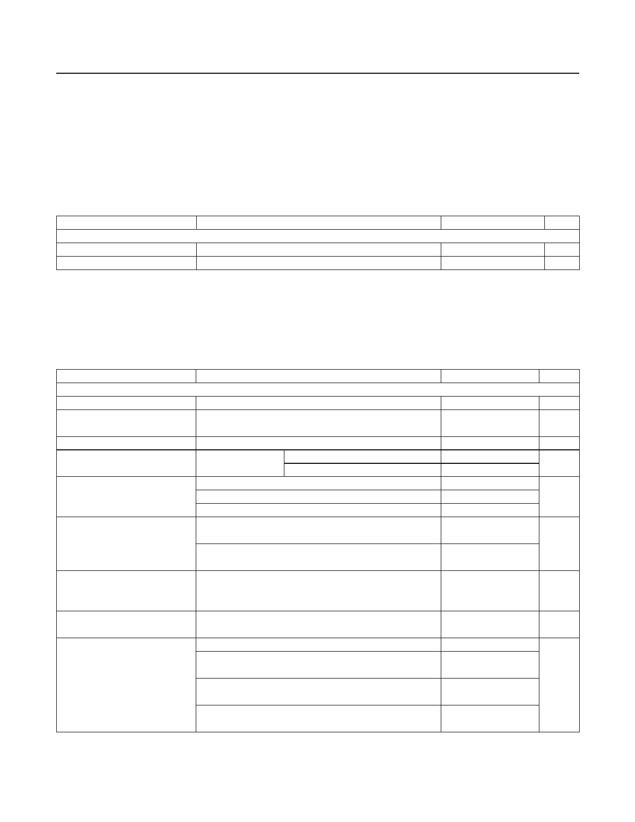
DC Electrical Characteristics (continued)
(MAX2837 evaluation kit: VCC_ = 2.7V to 3.6V, Rx set to the maximum gain; CS = high, RXHP = SCLK = DIN = low, RSSI and clock
output buffer are off, no signal at RF inputs, all RF inputs and outputs terminated into 50Ω, receiver baseband outputs are open;
90mVRMS differential I and Q signals applied to I, Q baseband inputs of transmitter in transmit mode, fREF = 40MHz, registers set to
recommended settings and corresponding test mode, TA = -40°C to +85°C, unless otherwise noted. Typical values are at VCC = 2.8V,
fLO = 2.5GHz, and TA = +25°C, unless otherwise noted.) (Note 1)
PARAMETER
CONDITIONS
MIN TYP MAX UNITS
LOGIC OUTPUTS: DOUT
Digital Output-Voltage High, VOH Sourcing 100µA
Digital Output-Voltage Low, VOL Sinking 100µA
VCC - 0.4
V
0.4
V
AC Electrical Characteristics—Rx MODE
(MAX2837 evaluation kit: VCC_ = 2.8V, fRF = 2.502GHz, fLO = 2.5GHz; receiver baseband I/Q outputs at 90mVRMS (-21dBV), fREF
= 40MHz, ENABLE = RXENABLE = CS = high, TXENABLE = SCLK = DIN = low, with power matching for the differential RF pins
using the typical applications and registers set to default settings and corresponding test mode, TA = +25°C, unless otherwise noted.
Lowpass filter is set to 10MHz RF channel BW. Unmodulated single-tone RF input signal is used, unless otherwise indicated.) (Note 1)
PARAMETER
CONDITIONS
MIN
RECEIVER SECTION: LNA RF INPUT TO BASEBAND I/Q OUTPUTS
RF Input Frequency Range
2.3
Peak-to-Peak Gain Variation over
RF Input Frequency Range
Tested at band edges and band center
RF Input Return Loss
All LNA gain settings
Total Voltage Gain
Maximum gain, B7:B1 = 0000000
90
TA = -40°C to +85°C Minimum gain, B7:B1 = 1111111
From max RF gain to max RF gain - 8dB
RF Gain Steps
From max RF gain to max RF gain - 16dB
From max RF gain to max RF gain - 32dB
Gain Change Settling Time
Any RF or baseband gain change; gain settling to within
P1dB of steady state; RXHP = 1
Any RF or baseband gain change; gain settling to within
P0.1dB of steady state; RXHP = 1
Baseband Gain Range
Baseband Gain Minimum
Step Size
DSB Noise Figure
From maximum baseband gain (B5:B1 = 00000) to minimum
baseband gain (B5:B1 = 11111),
58
TA = -40°C to +85°C
Voltage gain R 65dB with max RF gain (B7:B6 = 00)
Voltage gain = 50dB with max RF gain - 8dB
(B7:B6 = 01)
Voltage gain = 45dB with max RF gain - 16dB
(B7:B6 = 10)
Voltage gain = 15dB with max RF gain - 32dB
(B7:B6 = 11)
TYP MAX UNITS
2.7 GHz
0.8
dB
13
dB
99
dB
5
13
8
16
dB
32
0.2
µs
2
62
66
dB
2
dB
2.3
5.5
dB
17
27
www.maximintegrated.com
Maxim Integrated │ 3
Share Link: 