LTC1338 Просмотр технического описания (PDF) - Linear Technology
Номер в каталоге
Компоненты Описание
производитель
LTC1338 Datasheet PDF : 8 Pages
| |||
LTC1338
WU
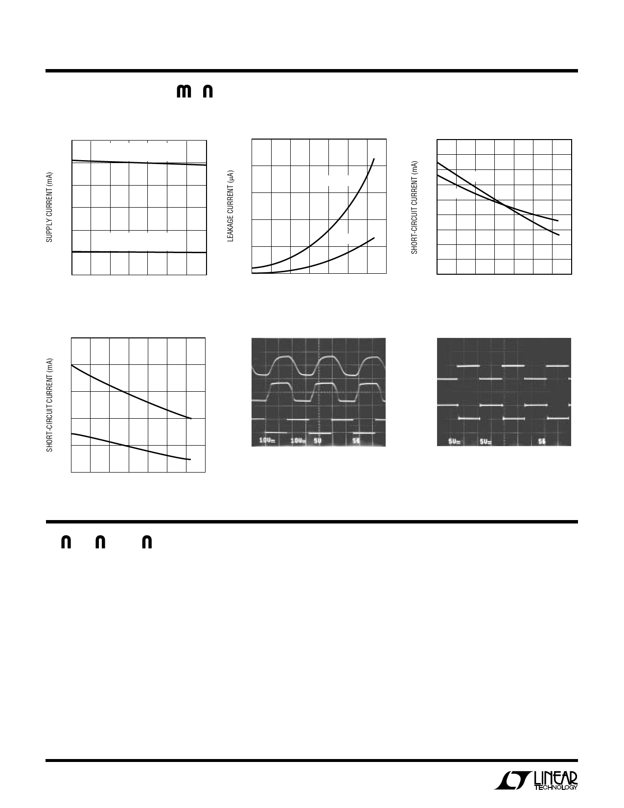
TYPICAL PERFOR A CE CHARACTERISTICS
VCC Supply Current
30
5 DRIVERS LOADED
RL = 3k
25
20
15
10
1 DRIVER LOADED
RL = 3k
5
0
–40 –20
0 20 40 60 80 100
TEMPERATURE (°C)
LTC1338 • TPC04
Driver Leakage in Shutdown
50
40
VOUT = –20V
30
20
VOUT = 20V
10
0
–40 –20
0 20 40 60 80 100
TEMPERATURE (°C)
LTC1338 • TPC05
Driver Short-Circuit Current
20
18
16
ISC–
14
ISC+
12
10
8
6
4
0
–40 –20
0 20 40 60 80 100
TEMPERATURE (°C)
LTC1338 • TPC06
Receiver Short-Circuit Current
60
50
40
ISC–
30
ISC+
20
Driver Output Waveforms
Receiver Output Waveforms
DRIVER
OUTPUT
RL = 3k
CL = 2500pF
DRIVER
OUTPUT
RL = 3k
INPUT
RECEIVER
OUTPUT
CL = 50pF
INPUT
LTC1338 • TPC08
LTC1338 • TPC09
10
–40 –20
0 20 40 60 80 100
TEMPERATURE (°C)
LTC1338 • TPC07
PI FU CTIO S
VCC: 5V Input Supply Pin. Supply current less than 0.2µA
in the SHUTDOWN mode. This pin should be decoupled
with a 0.1µF ceramic capacitor.
GND: Ground Pin.
RECEIVER ENABLE: TTL/CMOS Compatible Enable Pin.
Refer to Table 1 for its functional description. This pin can
not float.
DRIVER ENABLE: TTL/CMOS Compatible Enable Pin. Re-
fer to Table 1 for its functional description. This pin can not
float.
V+: Positive Supply Output (RS232 Drivers). V+ ≅ 2VCC –
1V. This pin requires an external capacitor C = 0.1µF for
charge storage. The capacitor may be tied to ground or 5V.
With multiple devices, the V + and V – pins may be paral-
leled into common capacitors. For large numbers of
devices, increasing the size of the shared common storage
capacitors is recommended to reduce ripple.
V–: Negative Supply Output (RS232 Drivers). V – ≅ 2VCC
– 1.5V. This pin requires an external capacitor C = 0.1µF for
charge storage.
C1+, C1–, C2+, C2–: Commutating Capacitor Inputs. These
pins require two external capacitors C = 0.1µF: one from
C1+ to C1–, and another from C2+ to C2–. To maintain
charge pump efficiency, the capacitor’s effective series
resistance should be less than 20Ω.
4
Share Link: 