M80C186XL Просмотр технического описания (PDF) - Intel
Номер в каталоге
Компоненты Описание
производитель
M80C186XL Datasheet PDF : 44 Pages
| |||
M80C186XL
Symbol
LOCK
PGA
Pin No
48
S0
52
S1
53
S2
54
HOLD
50
HLDA
51
UCS
34
LCS
33
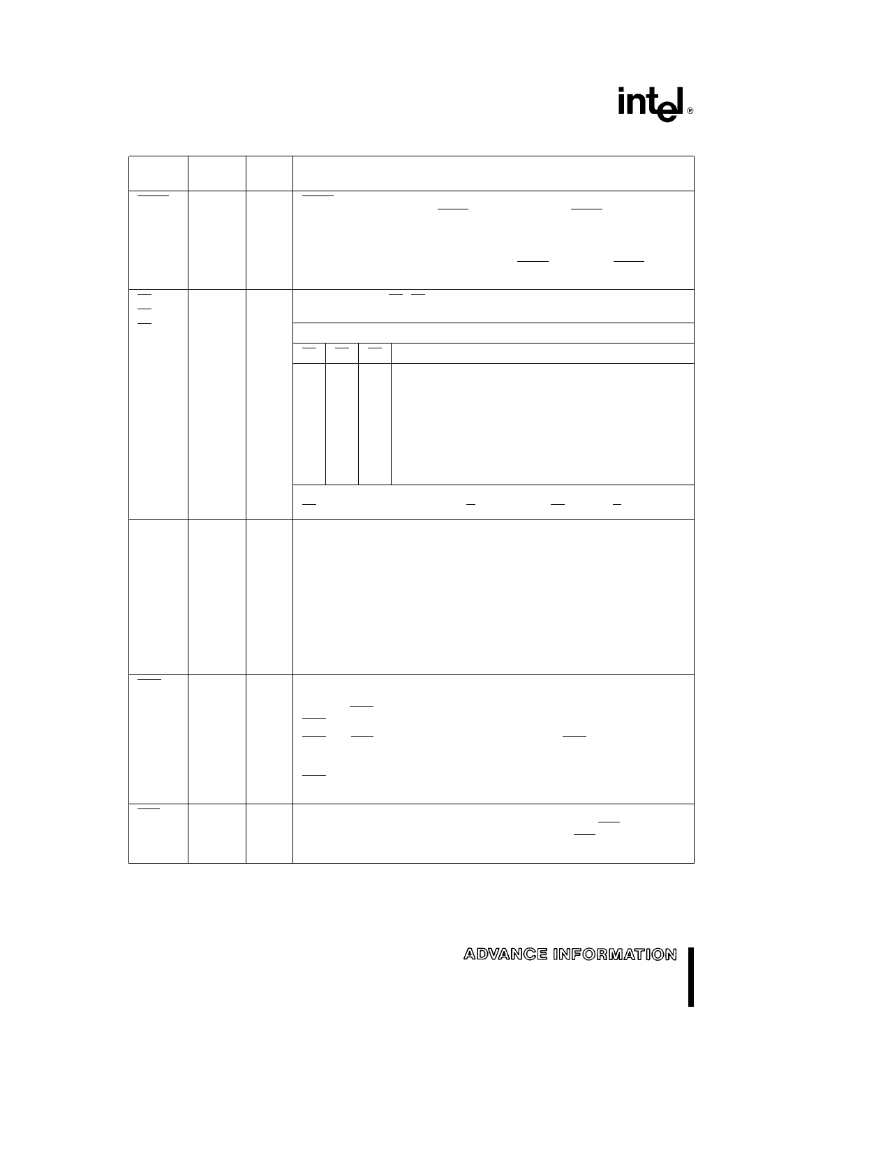
Table 1 M80C186XL Pin Description (Continued)
Type
Name and Function
O LOCK output indicates that other system bus masters are not to gain
control of the system bus LOCK is active LOW The LOCK signal is
requested by the LOCK prefix instruction and is activated at the beginning
of the first data cycle associated with the instruction immediately following
the LOCK prefix It remains active until the completion of that instruction
No instruction prefetching will occur while LOCK is asserted LOCK floats
during bus hold or reset
O Bus cycle status S0 –S2 are encoded to provide bus-transaction
O information
O
M80C186XL Bus Cycle Status Information
S2 S1 S0
Bus Cycle Initiated
0 0 0 Interrupt Acknowledge
0 0 1 Read I O
0 1 0 Write I O
0 1 1 Halt
1 0 0 Instruction Fetch
1 0 1 Read Data from Memory
1 1 0 Write Data to Memory
1 1 1 Passive (no bus cycle)
The status pins float during HOLD
S2 may be used as a logical M IO indicator and S1 as a DT R indicator
I
HOLD indicates that another bus master is requesting the local bus The
O HOLD input is active HIGH The M80C186XL generates HLDA (HIGH) in
response to a HOLD request Simultaneous with the issuance of HLDA
the M80C186XL will float the local bus and control lines After HOLD is
detected as being LOW the M80C186XL will lower HLDA When the
M80C186XL needs to run another bus cycle it will again drive the local bus
and control lines
In Enhanced Mode HLDA will go low when a DRAM refresh cycle is
pending in the M80C186XL and an external bus master has control of the
bus It will be up to the external master to relinquish the bus by lowering
HOLD so that the M80C186XL may execute the refresh cycle
O I Upper Memory Chip Select is an active LOW output whenever a memory
reference is made to the defined upper portion (1K – 256K block) of
memory UCS does not float during bus hold The address range activating
UCS is software programmable
UCS and LCS are sampled upon the rising edge of RES If both pins are
held low the M80C186XL will enter ONCE Mode In ONCE Mode all pins
assume a high impedance state and remain so until a subsequent RESET
UCS has a weak internal pullup that is active during RESET to ensure that
the M80C186XL does not enter ONCE Mode inadvertently
O I Lower Memory Chip Select is active LOW whenever a memory reference is
made to the defined lower portion (1K – 256K) of memory LCS does not
float during bus HOLD The address range activating LCS is software
programmable
8
Share Link: 