M80C186XL12 Просмотр технического описания (PDF) - Intel
Номер в каталоге
Компоненты Описание
производитель
M80C186XL12 Datasheet PDF : 44 Pages
| |||
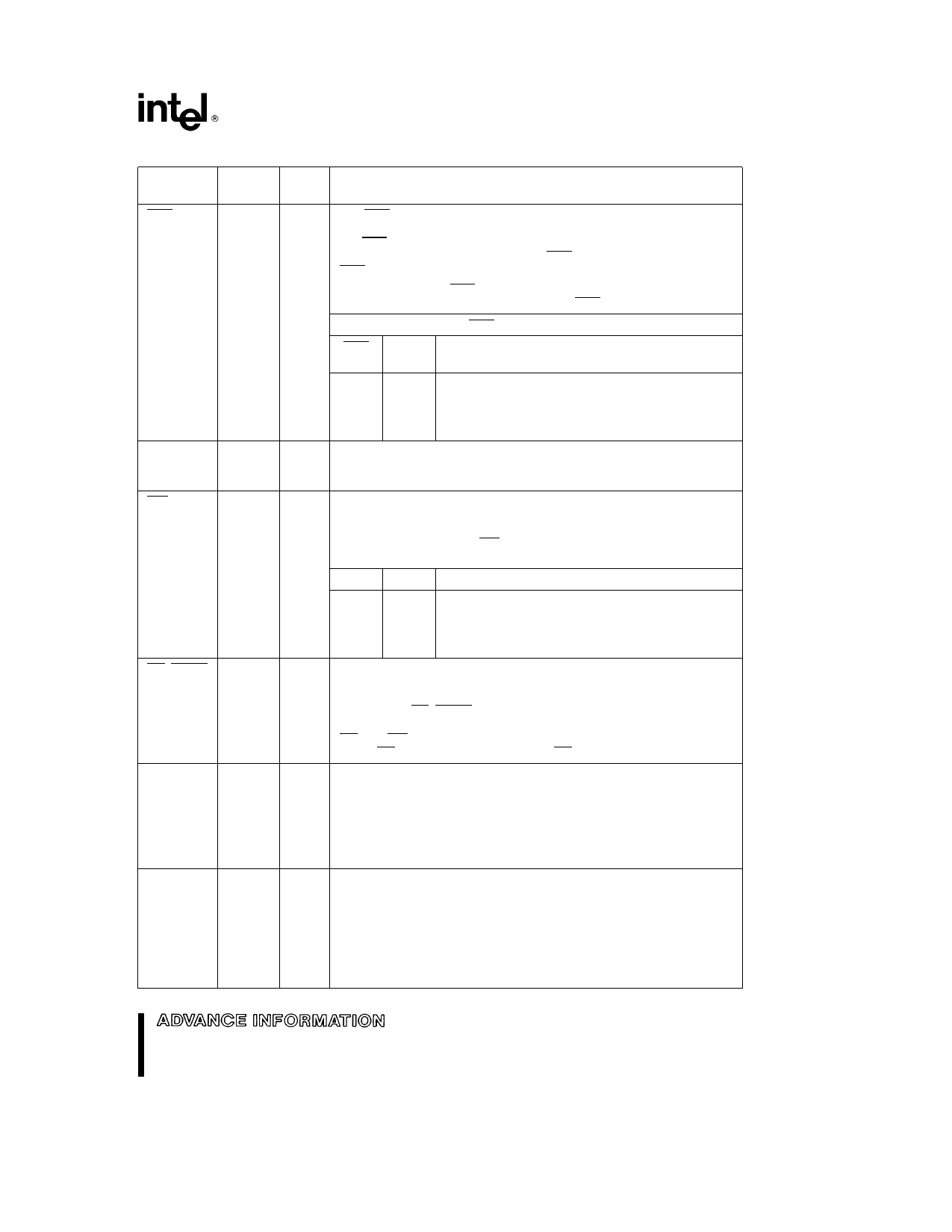
M80C186XL
Symbol
BHE
PGA
Pin No
64
ALE QS0
61
WR QS1
63
RD QSMD
62
ARDY
55
SRDY
49
Table 1 M80C186XL Pin Description (Continued)
Type
Name and Function
O The BHE (Bus High Enable) signal is analogous to A0 in that it is used
to enable data on to the most significant half of the data bus pins D15 –
D8 BHE will be LOW during T1 when the upper byte is transferred and
will remain LOW through T3 AND TW BHE does not need to be latched
BHE will float during HOLD or RESET
In Enhanced Mode BHE will also be used to signify DRAM refresh
cycles A refresh cycle is indicated by both BHE and A0 being HIGH
BHE and A0 Encodings
BHE
A0
Value Value
Function
0
0
Word Transfer
0
1
Byte Transfer on upper half of data bus (D15 – D8)
1
0
Byte Transfer on lower half of data bus (D7 – D0)
1
1
Refresh
O Address Latch Enable Queue Status 0 is provided by the M80C186XL
to latch the address ALE is active HIGH with addresses guaranteed
valid on the trailing edge
O Write Strobe Queue Status 1 indicates that the data on the bus is to be
written into a memory or an I O device It is active LOW and floats
during bus hold or reset When the M80C186XL is in Queue Status
Mode the ALE QS0 and WR QS1 pins provide information about
processor instruction queue interaction
QS1 QS0
Queue Operation
0
0
No queue operation
0
1
First opcode byte fetched from the queue
1
1
Subsequent byte fetched from the queue
1
0
Empty the queue
O I Read Strobe is an active LOW signal which indicates that the
M80C186XL is performing a memory or I O read cycle It is guaranteed
not to go LOW before the A D bus is floated An internal pull-up
ensures that RD QSMD is HIGH during RESET Following RESET the
pin is sampled to determine whether the M80C186XL is to provide ALE
RD and WR or queue status information To enable Queue Status
Mode RD must be connected to GND RD will float during bus HOLD
I
Asynchronous Ready informs the M80C186XL that the addressed
memory space or I O device will complete a data transfer The ARDY
pin accepts a rising edge that is asynchronous to CLKOUT and is active
HIGH The falling edge of ARDY must be synchronized to the
M80C186XL clock Connecting ARDY HIGH will always assert the
ready condition to the CPU If this line is unused it should be tied LOW
to yield control to the SRDY pin
I
Synchronous Ready informs the M80C186XL that the addressed
memory space or I O device will complete a data transfer The SRDY
pin accepts an active-HIGH input synchronized to CLKOUT The use of
SRDY allows a relaxed system timing over ARDY This is accomplished
by elimination of the one-half clock cycle required to internally
synchonize the ARDY input signal Connecting SRDY high will always
assert the ready condition to the CPU If this line is unused it should be
tied LOW to yield control to the ARDY pin
7
Share Link: 