M68AW511AL70MC1T Просмотр технического описания (PDF) - STMicroelectronics
Номер в каталоге
Компоненты Описание
производитель
M68AW511AL70MC1T Datasheet PDF : 21 Pages
| |||
M68AW511A
OPERATION
The M68AW511A has a Chip Enable power down
feature which invokes an automatic standby mode
whenever Chip Enable is de-asserted (E = High).
An Output Enable (G) signal provides a high
speed tri-state control, allowing fast read/write cy-
cles to be achieved with the common I/O data bus.
Operational modes are determined by device con-
trol inputs W and E as summarized in the Operat-
ing Modes table (Table 2).
Read Mode
The M68AW511A is in the Read mode whenever
Write Enable (W) is High with Output Enable (G)
Low, and Chip Enable (E) is asserted. This pro-
vides access to data from eight of the 4,194,304
locations in the static memory array, specified by
the 19 address inputs. Valid data will be available
at the eight output pins within tAVQV after the last
Write Mode
The M68AW511A is in the Write mode whenever
the W and E pins are Low. Either the Chip Enable
input (E) or the Write Enable input (W) must be de-
asserted during Address transitions for subse-
quent write cycles. Write begins with the concur-
rence of Chip Enable being active with W low.
Therefore, address setup time is referenced to
Write Enable and Chip Enable as tAVWL and tAVEH
respectively, and is determined by the latter occur-
ring edge.
stable address, providing G is Low and E is Low.
If Chip Enable or Output Enable access times are
not met, data access will be measured from the
limiting parameter (tELQV or tGLQV) rather than the
address. Data out may be indeterminate at tELQX
and tGLQX, but data lines will always be valid at
tAVQV.
The Write cycle can be terminated by the earlier
rising edge of E, or W.
if the Output is enabled (E = Low and G = Low),
then W will return the outputs to high impedance
within tWLQZ of its falling edge. Care must be taken
to avoid bus contention in this type of operation.
Data input must be valid for tDVWH before the ris-
ing edge of Write Enable, or for tDVEH before the
rising edge of E, whichever occurs first, and re-
main valid for tWHDX or tEHDX.
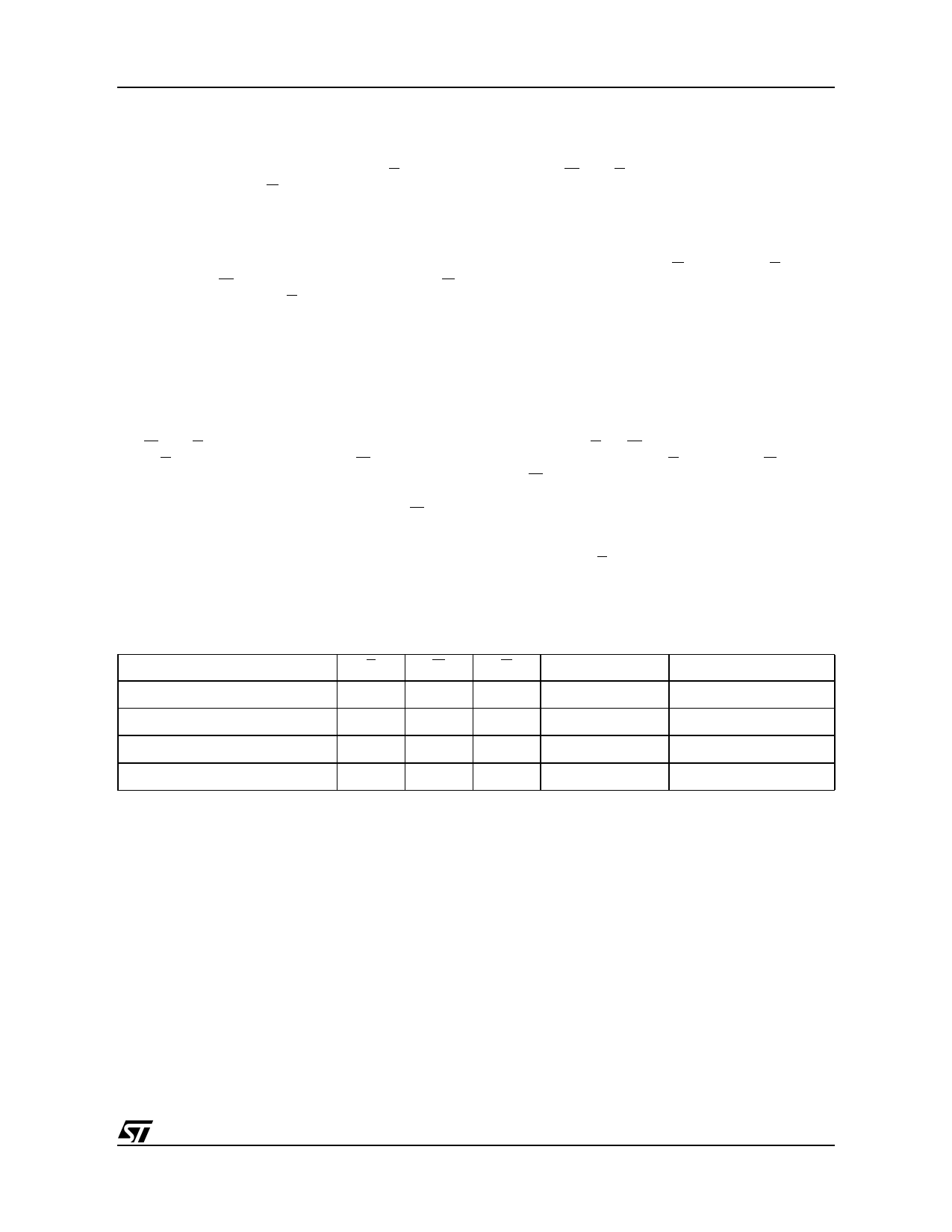
Table 2. Operating Modes
Operation
Output Disabled
Read
Write
Deselect
Note: X = VIH or VIL.
E
W
G
VIL
X
VIH
VIL
VIH
VIL
VIL
VIL
X
VIH
X
X
DQ0-DQ7
Hi-Z
Data Output
Data Input
Hi-Z
Power
Active (ICC)
Active (ICC)
Active (ICC)
Standby (ISB)
7/21
Share Link: 