M64611FP Просмотр технического описания (PDF) - Renesas Electronics
Номер в каталоге
Компоненты Описание
производитель
M64611FP Datasheet PDF : 7 Pages
| |||
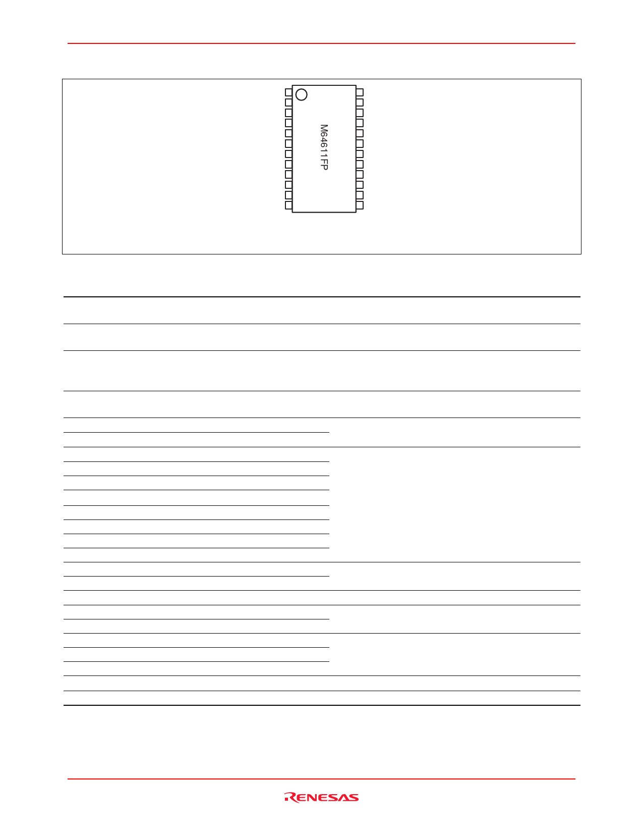
M64611FP
Pin Arrangement
Vreg
DAO
Neutral
Vcc
OUT1
OUT2
MD1
MD2
BT1
BT2
ST1
ST2
GND
POT
Rop1
Rop3
Rop2
DMP-
DMP+
Pin
CL1
CL2
DB1
DB2
Outline : 24P2E
Pin Description
Pin No. Symbol
1
Vreg
Function
Regulated voltage output
2
DAO
D/A converter output
3
Neutral Neutral voltage output
4
Vcc
Supply voltage
5
OUT1
Output pin 1
6
OUT2
Output pin 2
7
MD1
Max. duty input 1
8
MD2
Max. duty input 2
9
BT1
Boost input 1
10
BT2
Boost input 2
11
ST1
Stretcher input 1
12
ST2
Stretcher input 2
13
DB2
Dead Band input 2
14
DB1
Dead Band input 1
15
CL2
Oscillation terminal 2
16
CL1
Oscillation terminal 1
17
Pin
Receiving pulse input
18
DMP+
Damping resistor input+
19
DMP-
Damping resistor input-
20
ROP2
Gain Adjustment Resistor 2
21
ROP3
Gain Adjustment Resistor 3
22
ROP1
Gain Adjustment Resistor 1
23
POT
Servo position voltage input
24
GND
GND
Notes
Connect a capacitor for the stabilization between Vreg
and GND
Connect the capacitor for the filter of 100 – 1000pF
between DAO and GND.
Make it open usually.
Connect a capacitor for the stabilization between Neutral
and GND if Neutral voltage is unstable.
Connect the Electrolytic condenser more than 10 µF and
the ceramics condenser more than 0.1 µF.
Connect to the external driver IC for servo drive.
Refer to the following input table.
When it is “H” : OPEN
When it is “L” : GND
Connect to resonator between CL1 and CL2.
Connect to the damping resistor of 100 k Ω -1 MΩ.
Connect to the resistances for adjusting Gain.
Connect the potentiometer.
Rev.1.00, Aug.26.2003, page 2 of 6
Share Link: 