M35052 Просмотр технического описания (PDF) - Mitsumi
Номер в каталоге
Компоненты Описание
производитель
M35052 Datasheet PDF : 36 Pages
| |||
MITSUBISHI MICROCOMPUTERS
M35052-XXXSP/FP
SCREEN CHARACTER and PATTERN DISPLAY CONTROLLERS
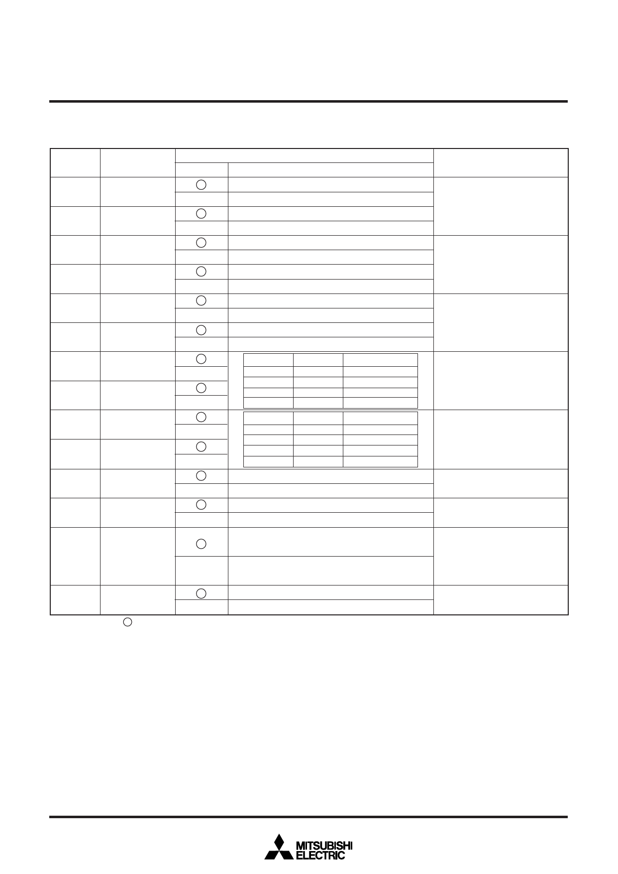
Display control register
(1) Address F016
DA
Register
0~D
0
PTC0
1
PTC1
2
PTD0
3
PTD1
4
SEPV0
5
SEPV1
6
SYSEP0
7
SYSEP1
8
DECB0
9
DECB1
A
TEST10
B
TEST11
Status
0
1
0
1
0
1
0
1
0
1
0
1
0
1
0
1
0
1
0
1
0
1
0
1
0
____
C
W/R
1
Contents
Function
Remarks
P0 output (port 0)
Port output control
BLNK1 output
P1 output (port 1)
CO1 output
Refer to supplemental explanation (5).
It is negative polarity at P0 output “L”, BLINK1 output. Control the port data
It is positive polarity at P0 output “H”, BLINK1 output.
It is negative polarity at P01 output “L”, CO1 output.
It is positive polarity at P01 output “H”, CO1 output. Refer to supplemental explanation (5).
It should be fixed to “0”.
Can not be used.
Specifies the vertical synchronous
separation criterion
It should be fixed to “0”.
Can not be used.
Refer to supplemental explanation (1).
SYSEP1
0
0
1
1
SYSEP0
0
1
0
1
Bias potential
Can not be used.
Can not be used.
1.75µ
Can not be used.
Specifies the sync-bias potential
DECB1
0
0
1
1
DECB0
0
1
0
1
Bias potential
2.35µ
Can not be used.
Can not be used.
Can not be used.
Specifies the decoding bias
potential
Can not be used.
It should be fixed to “1”.
It should be fixed to “0”.
Can not be used.
Input data from SIN pin
Control data I/O
Output data from SIN pin (Note 2)
Refer to decode data output
timing.
D
TEST25
0
It should be fixed to “0”.
1
Can not be used.
__
Notes 1. The mark around the status value means the reset status by the “L” level is input to AC pin.
__
___
Notes 2. Not necessary to release after setting W/R to “1”. Turn CS to “H” to switch over to input mode.
7
Share Link: 