M28C64 Просмотр технического описания (PDF) - STMicroelectronics
Номер в каталоге
Компоненты Описание
производитель
M28C64 Datasheet PDF : 24 Pages
| |||
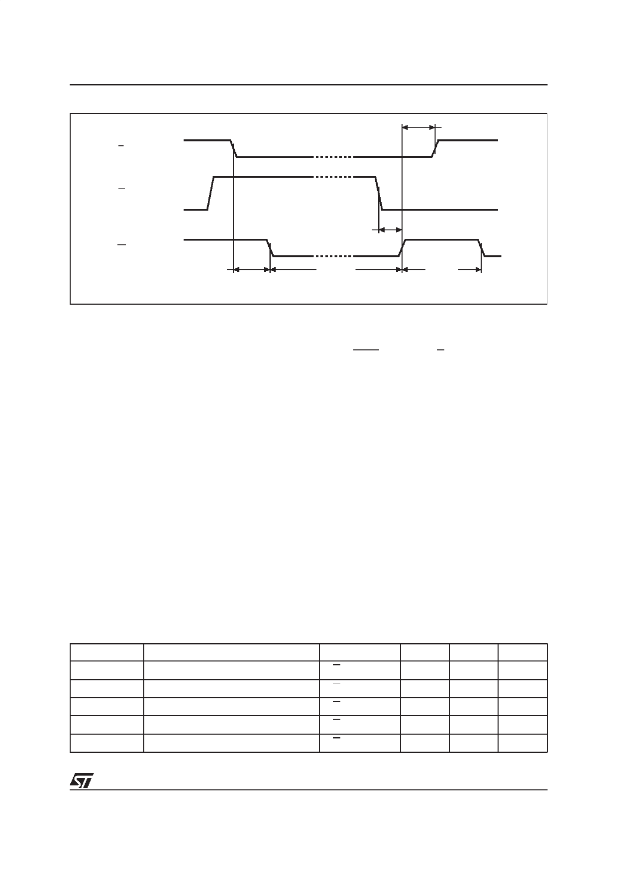
Figure 7. Chip Erase AC Waveforms (M28C64 and M28C64-xxW)
E
M28C64
tWHEH
G
W
tELWL
tGLWH
tWLWH2
tWHRH
AI01484B
throughout this write operation: it is inverted while
the internal write operation is underway, and is
inverted back to its original value once the
operation is complete.
Toggle bit (DQ6). The device offers another way
for determining when the internal write cycle is
completed. During the internal Erase/Write cycle,
DQ6 toggles from ’0’ to ’1’ and ’1’ to ’0’ (the first
read value being ’0’) on subsequent attempts to
read any byte of the memory. When the internal
write cycle is complete, the toggling is stopped,
and the values read on DQ7-DQ0 are those of the
addressed memory byte. This indicates that the
device is again available for new Read and Write
operations.
Page Load Timer Status bit (DQ5). An internal
timer is used to measure the period between
successive Write operations, up to tWLQ5H
(defined in Table 10A to Table 10C). The DQ5 line
is held low to show when this timer is running
(hence showing that the device has received one
write operation, and is waiting for the next). The
DQ5 line is held high when the counter has
overflowed (hence showing that the device is now
starting the internal write to the memory array).
Ready/Busy pin. The RB pin is an open drain
output that is held low during the erase/write cycle,
and that is released (allowed to float) at the
completion of the programming cycle.
Table 5. Chip Erase AC Characteristics1 for M28C64 and M28C64-xxW
(TA = 0 to 70 °C or –40 to 85 °C or –40 to 125 °C; VCC = 4.5 to 5.5 V)
(TA = 0 to 70 °C or –40 to 85 °C; VCC = 2.7 to 3.6 V)
Symbol
Parameter
Test Condition
Min.
tELWL
Chip Enable Low to Write Enable Low
G = VCC + 7V
1
tWHEH
Write Enable High to Chip Enable High
G = VCC + 7V
0
tWLWH2
Write Enable Low to Write Enable High
G = VCC + 7V
10
tGLWH
Output Enable Low to Write Enable High
G = VCC + 7V
1
tWHRH
Write Enable High to Write Enable Low
Note: 1. Sampled only, not 100% tested.
G = VCC + 7V
Max.
3
Unit
µs
ns
ms
µs
ms
7/24
Share Link: 