AM27X512 Просмотр технического описания (PDF) - Advanced Micro Devices
Номер в каталоге
Компоненты Описание
производитель
AM27X512 Datasheet PDF : 10 Pages
| |||
FUNCTIONAL DESCRIPTION
Read Mode
To obtain data at the device outputs, Chip Enable (CE#)
and Output Enable (OE#) must be driven low. CE# con-
trols the power to the device and is typically used to se-
lect the device. OE# enables the device to output data,
independent of device selection. Addresses must be
stable for at least tACC–tOE. Refer to the Switching
Waveforms section for the timing diagram.
Standby Mode
The device enters the CMOS standby mode when CE#
is at VCC ± 0.3 V. Maximum VCC current is reduced to
100 µA. The device enters the TTL-standby mode
when CE# is at VIH. Maximum VCC current is reduced
to 1.0 mA. When in either standby mode, the device
places its outputs in a high-impedance state, indepen-
dent of the OE# input.
Output OR-Tieing
To accommodate multiple memory connections, a
two-line control function provides:
s Low memory power dissipation, and
s Assurance that output bus contention will not occur.
CE# should be decoded and used as the primary de-
vice-selecting function, while OE#/VPP be made a com-
mon connection to all devices in the array and
connected to the READ line from the system control
bus. This assures that all deselected memory devices
are in their low-power standby mode and that the out-
put pins are only active when data is desired from a
particular memory device.
System Applications
During the switch between active and standby condi-
tions, transient current peaks are produced on the ris-
ing and falling edges of Chip Enable. The magnitude of
these transient current peaks is dependent on the out-
put capacitance loading of the device. At a minimum, a
0.1 µF ceramic capacitor (high frequency, low inherent
inductance) should be used on each device between
VCC and VSS to minimize transient effects. In addition,
to overcome the voltage drop caused by the inductive
effects of the printed circuit board traces on Express-
ROM device arrays, a 4.7 µF bulk electrolytic capacitor
should be used between VCC and VSS for each eight
devices. The location of the capacitor should be close
to where the power supply is connected to the array.
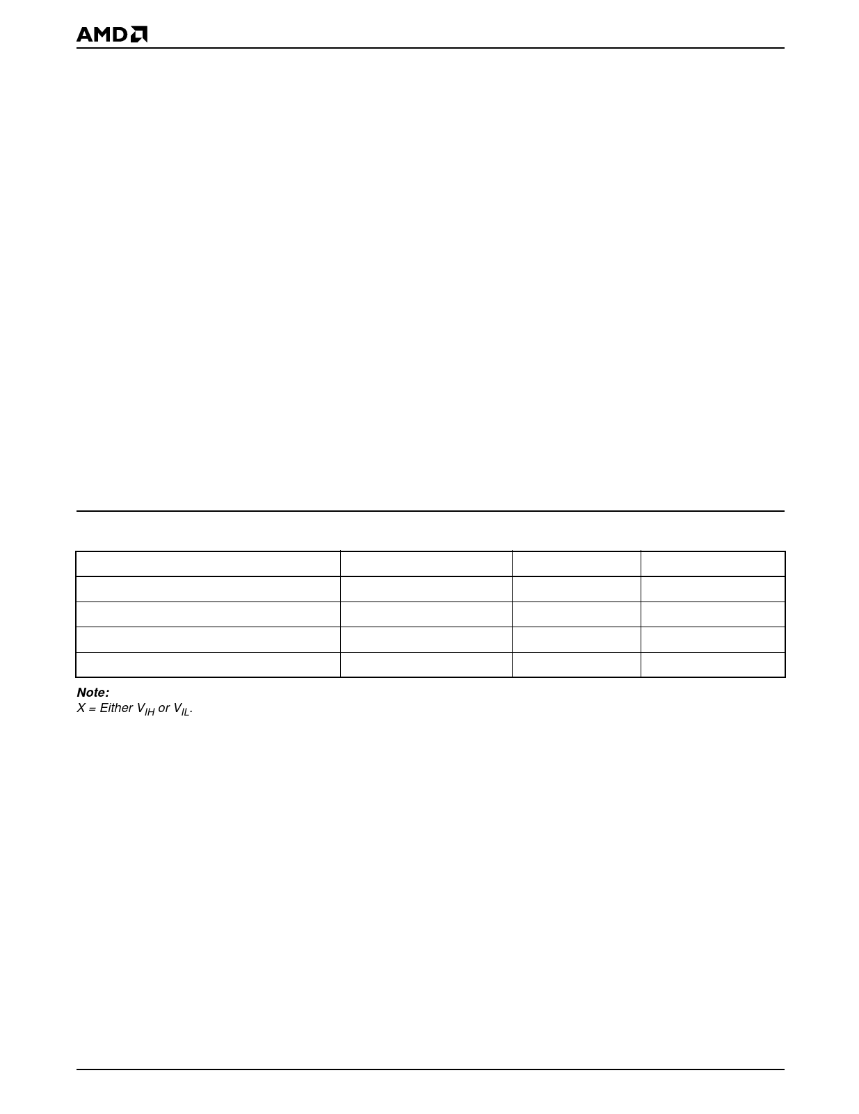
MODE SELECT TABLE
Mode
Read
Output Disable
Standby (TTL)
Standby (CMOS)
Note:
X = Either VIH or VIL.
CE#
VIL
X
VIH
VCC ± 0.3 V
OE#/VPP
VIL
VIH
X
X
Outputs
DOUT
High Z
High Z
High Z
4
Am27X512
Share Link: 