LTM4614(RevA) –Я—А–Њ—Б–Љ–Њ—В—А —В–µ—Е–љ–Є—З–µ—Б–Ї–Њ–≥–Њ –Њ–њ–Є—Б–∞–љ–Є—П (PDF) - Linear Technology
–Э–Њ–Љ–µ—А –≤ –Ї–∞—В–∞–ї–Њ–≥–µ
–Ъ–Њ–Љ–њ–Њ–љ–µ–љ—В—Л –Ю–њ–Є—Б–∞–љ–Є–µ
–њ—А–Њ–Є–Ј–≤–Њ–і–Є—В–µ–ї—М
LTM4614 Datasheet PDF : 20 Pages
| |||
LTM4614
APPLICATIONS INFORMATION
Dual Switching Regulator
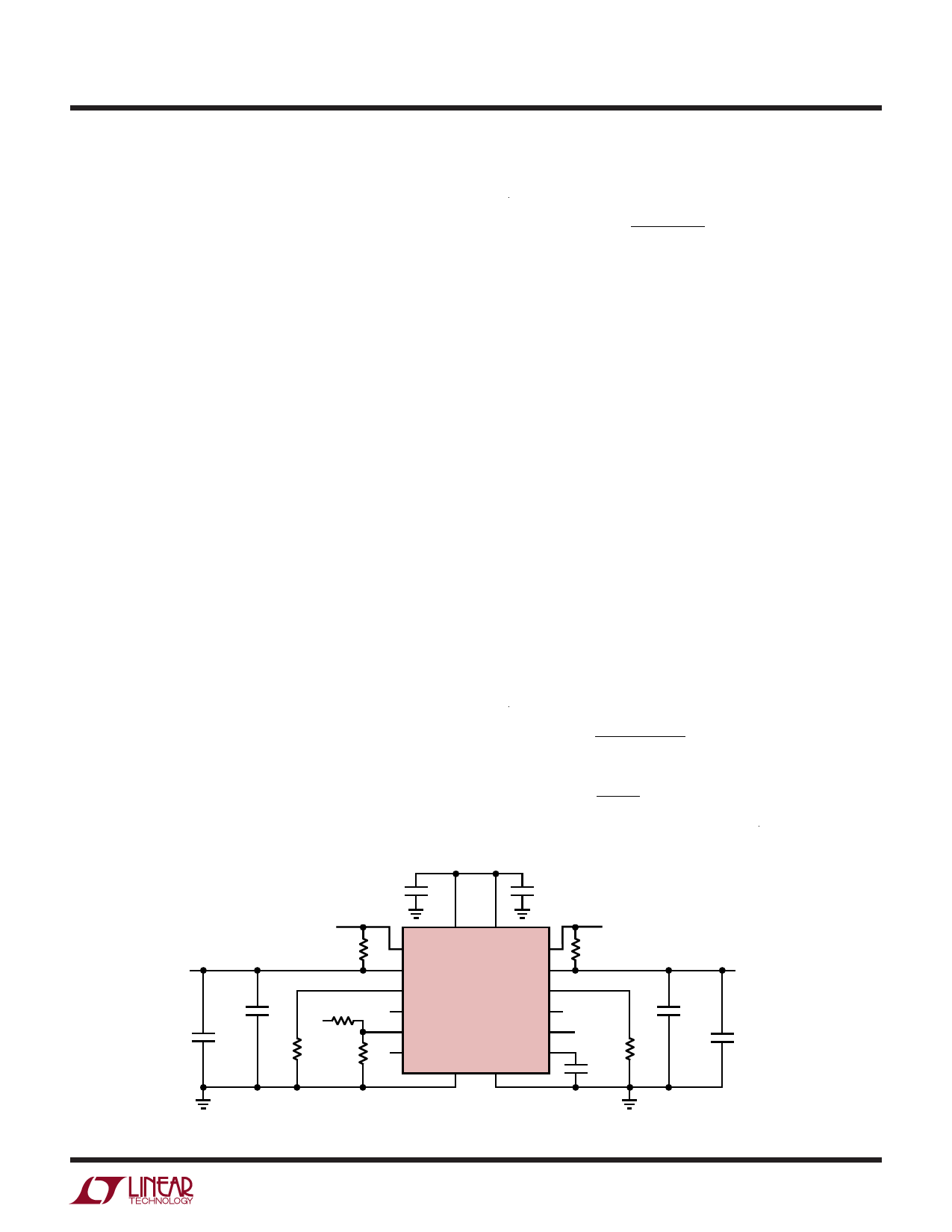
A typical LTM4614 application circuit is shown in Figure 12.
External component selection is primarily determined by
the maximum load current and output voltage. Refer to
Table 4 for speciпђБc external capacitor requirements for a
particular application.
VIN to VOUT Step-Down Ratios
There are restrictions in the maximum VIN and VOUT step-
down ratio than can be achieved for a given input voltage
on the two switching regulators. The LTM4614 is 100%
duty cycle, but the VIN to VOUT minimum dropout will be
a function the load current. A typical 0.5V minimum is
sufпђБcient.
Output Voltage Programming
Each regulator channel has an internal 0.8V reference
voltage. As shown in the Block Diagram, a 4.99k internal
feedback resistor connects the VOUT and FB pins together.
The output voltage will default to 0.8V with no feedback
resistor. Adding a resistor RFB from the FB pin to GND
programs the output voltage:
VOUT
=
0.8V
вАҐ
4.99k +
RFB
RFB
Table 1. FB Resistor Table vs Various Output Voltages
VOUT 0.8V 1.2V 1.5V 1.8V 2.5V
RFB Open 10k 5.76k 3.92k 2.37k
3.3V
1.62k
Input Capacitors
The LTM4614 module should be connected to a low AC
impedance DC source. One 4.7ќЉF ceramic capacitor is
included inside the module for each regulator channel.
Additional input capacitors are needed if a large load step
is required up to the full 4A level and for RMS ripple cur-
rent requirements. A 47ќЉF bulk capacitor can be used for
more input bulk capacitance. This 47ќЉF capacitor is only
needed if the input source impedance is compromised by
long inductive leads or traces.
For a buck converter, the switching duty cycle can be
estimated as:
D = VOUT
VIN
Without considering the inductor current ripple, the RMS
current of the input capacitor can be estimated as:
( ) ICIN(RMS)
=
IOUT(MAX )
ќЈ%
вАҐ
D вАҐ 1вАУ D
In the above equation, ќЈ% is the estimated efпђБciency of
the power module. The bulk capacitor can be a switcher-
rated electrolytic aluminum OS-CON capacitor for bulk
input capacitance due to high inductance traces or leads.
If a low inductance plane is used to power the device,
then no input capacitance is required. The internal 4.7ќЉF
ceramics on each channel input are typically rated for 1A of
RMS ripple current up to 85°C operation. The worst-case
ripple current for the 4A maximum current is 2A or less.
An additional 10ќЉF or 22ќЉF ceramic capacitor can be used
to supplement the internal capacitor with an additional 1A
to 2A ripple current rating.
Output Capacitors
The LTM4614 switchers are designed for low output volt-
age ripple on each channel. The bulk output capacitors are
chosen with low enough effective series resistance (ESR)
to meet the output voltage ripple and transient require-
ments. The output capacitors can be a low ESR tantalum
capacitor, low ESR polymer capacitor or ceramic capacitor.
The typical output capacitance range is 66ќЉF to 100ќЉF.
Additional output пђБltering may be required by the system
designer, if further reduction of output ripple or dynamic
transient spike is required. Table 4 shows a matrix of dif-
ferent output voltages and output capacitors to minimize
the voltage droop and overshoot during a 2A/ќЉs transient.
The table optimizes total equivalent ESR and total bulk
capacitance to maximize transient performance.
4614fa
9
Share Link: 