LTM2882 –ü—Ä–æ—Å–º–æ—Ç—Ä —Ç–µ—Ö–Ω–∏—á–µ—Å–∫–æ–≥–æ –æ–ø–∏—Å–∞–Ω–∏—è (PDF) - Linear Technology
–ù–æ–º–µ—Ä –≤ –∫–∞—Ç–∞–ª–æ–≥–µ
–ö–æ–º–ø–æ–Ω–µ–Ω—Ç—ã –û–ø–∏—Å–∞–Ω–∏–µ
–ø—Ä–æ–∏–∑–≤–æ–¥–∏—Ç–µ–ª—å
LTM2882 Datasheet PDF : 22 Pages
| |||
LTM2882
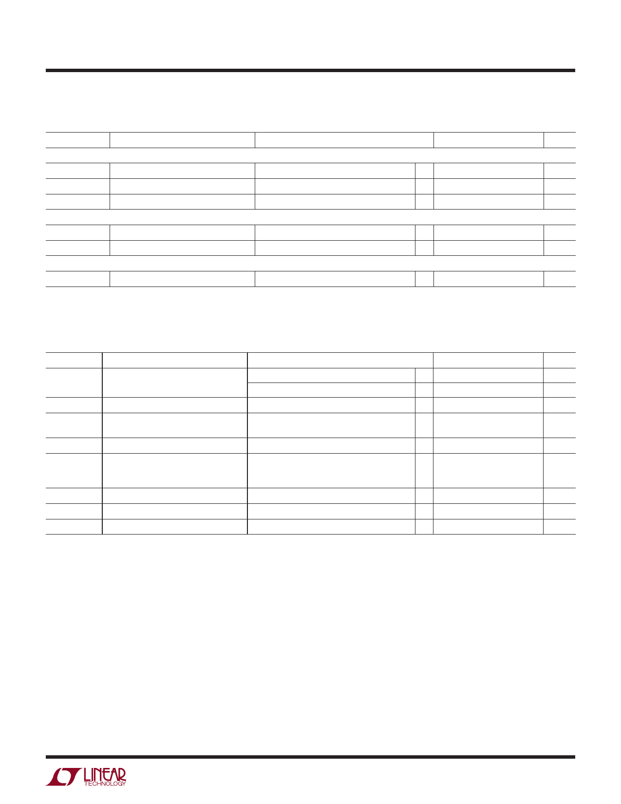
switching Characteristics The l denotes the specifications which apply over the full operating
temperature range, otherwise specifications are at TA = 25°C. LTM2882-3 VCC = 3.3V, LTM2882-5 VCC = 5.0V, VL = VCC, and GND =
GND2 = 0V, ON = VL unless otherwise noted.
SYMBOL
PARAMETER
Receiver
tPHLR, tPLHR
Receiver Propagation Delay
tSKEWR
Receiver Skew |tPHLR – tPLHR|
tRR, tFR
Receiver Rise or Fall Time
Auxiliary Channel
tPHLL, tPLHL
tRL, tFL
Power Supply
Propagation Delay
Rise or Fall Time
Power-Up Time
CONDITIONS
CL = 150pF (Figure 3)
CL = 150pF (Figure 3)
CL = 150pF (Figure 3)
CL = 15pF, tR and tF < 4ns (Figure 4)
CL = 150pF (Figure 4)
ON = ‚Üë to VCC2(MIN)
MIN TYP MAX UNITS
l
0.2
0.4
µs
40
ns
l
60
200
ns
l
60
100
ns
l
60
200
ns
l
0.2
2
ms
Isolation Characteristics The l denotes the specifications which apply over the full operating
temperature range, otherwise specifications are at TA = 25°C. LTM2882-3 VCC = 3.3V, LTM2882-5 VCC = 5.0V, VL = VCC, and GND =
GND2 = 0V, ON = VL unless otherwise noted.
SYMBOL
PARAMETER
CONDITIONS
MIN TYP MAX UNITS
VISO
Rated Dielectric Insulation Voltage
1 Minute, Derived from 1 Second Test
1 Second (Notes 5, 6)
2500
±4400
VRMS
V
Common Mode Transient Immunity
VL = ON = 3.3V, VCM = 1kV, ∆t = 33ns (Note 2)
30
kV/µs
VIORM
Maximum Working Insulation Voltage (Notes 2, 5)
Partial Discharge
VPR = 1050 VPEAK (Notes 2, 5)
560
VPEAK
400
VRMS
5
pC
CTI
Comparative Tracking Index
IEC 60112 (Note 2)
DTI
Depth of Erosion
IEC 60112 (Note 2)
Distance Through Insulation
(Note 2)
Input to Output Resistance
(Notes 2, 5)
600
0.017
0.06
109
VRMS
mm
mm
Ω
Input to Output Capacitance
(Notes 2, 5)
6
pF
Creepage Distance
(Notes 2, 5)
9.48
mm
Note 1: Stresses beyond those listed under Absolute Maximum Ratings
may cause permanent damage to the device. Exposure to any Absolute
Maximum Rating condition for extended periods may affect device
reliability and lifetime.
Note 2: Guaranteed by design and not subject to production test.
Note 3: Maximum Data Rate is guaranteed by other measured parameters
and is not tested directly.
Note 4: This device includes over-temperature protection that is intended
to protect the device during momentary overload conditions. Junction
temperature will exceed 105°C when overtemperature protection is active.
Continuous operation above specified maximum operating junction
temperature may result in device degradation or failure.
Note 5: Tests performed from GND to GND2, all pins shorted each side of
isolation barrier.
Note 6: The rated dielectric insulation voltage should not be interpreted as
a continuous voltage rating.
2882ff
For more information www.linear.com/LTM2882
5
Share Link: 