LTC693I Просмотр технического описания (PDF) - Linear Technology
Номер в каталоге
Компоненты Описание
производитель
LTC693I Datasheet PDF : 16 Pages
| |||
LTC692/LTC693
APPLICATI S I FOR ATIO
Microprocessor Reset
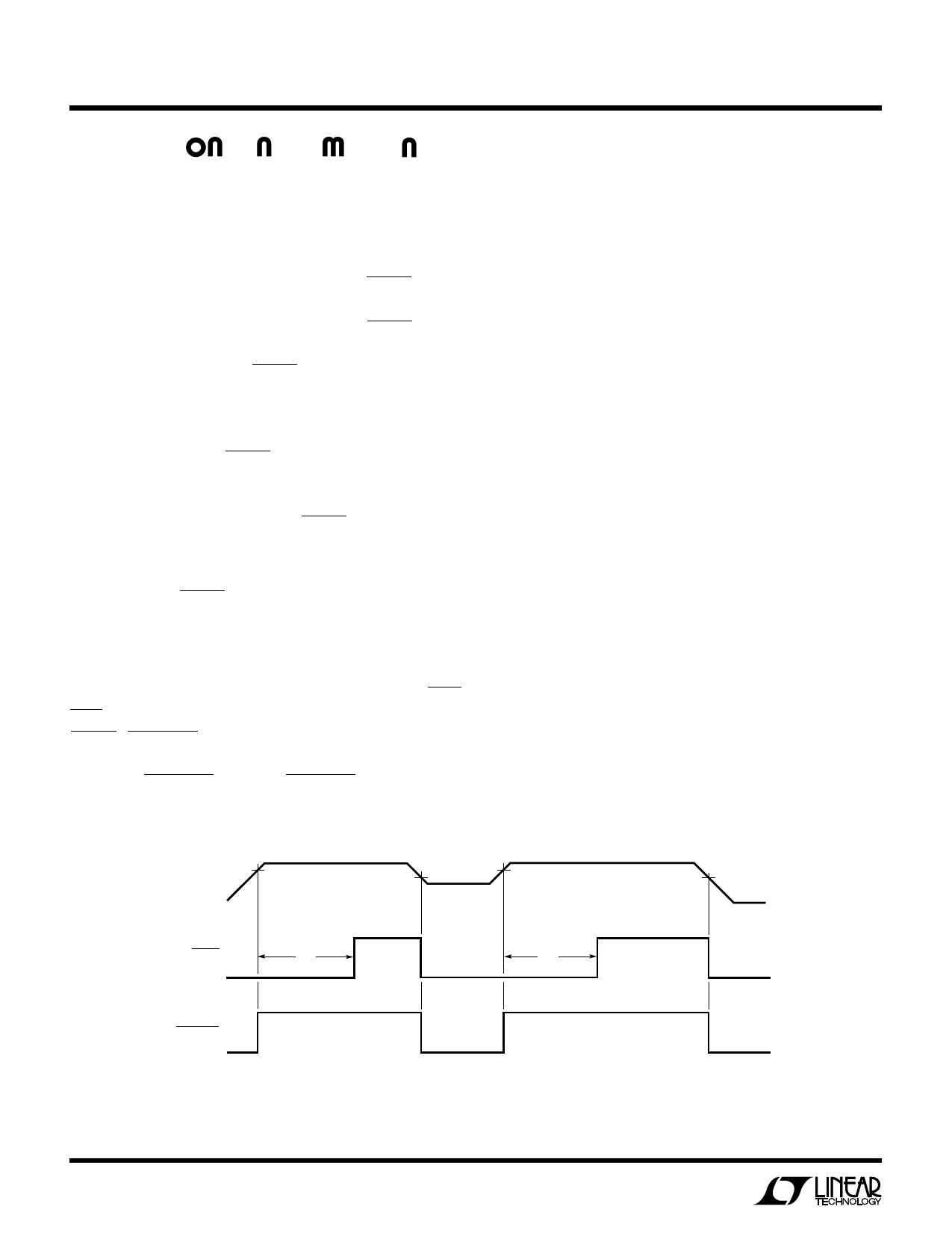
The LTC692/LTC693 use a bandgap voltage reference and
a precision voltage comparator C1 to monitor the 5V
supply input on VCC (see BLOCK DIAGRAM). When VCC
falls below the reset voltage threshold, the RESET output
is forced to active low state. The reset voltage threshold
accounts for a 10% variation on VCC, so the RESET output
becomes active low when VCC falls below 4.50V (4.40V
typical). On power-up, the RESET signal is held active low
for a minimum of 140ms after reset voltage threshold is
reached to allow the power supply and microprocessor to
stabilize. The reset active time is adjustable on the LTC693.
On power-down, the RESET signal remains active low
even with VCC as low as 1V. This capability helps hold the
microprocessor in stable shutdown condition. Figure 1
shows the timing diagram of the RESET signal.
The precision voltage comparator, C1, typically has 40mV
of hysteresis which ensures that glitches at the VCC pin do
not activate the RESET output. Response time is typically
10µs. To help prevent mistriggering due to transient loads,
VCC pin should be bypassed with a 0.1µF capacitor with the
leads trimmed as short as possible.
The LTC693 has two additional outputs: RESET and LOW
LINE. RESET is an active high output and is the inverse of
RESET. LOW LINE is the output of the precision voltage
comparator C1. When VCC falls below the reset voltage
threshold, LOW LINE goes low. LOW LINE returns high as
soon as VCC rises above the reset voltage threshold.
Battery Switchover
The battery switchover circuit compares VCC to the
VBATT input, and connects VOUT to whichever is higher.
When VCC rises to 70mV above VBATT, the battery
switchover comparator, C2, connects VOUT to VCC through
a charge pumped NMOS power switch, M1. When VCC
falls to 50mV above VBATT, C2 connects VOUT to VBATT
through a PMOS switch, M2. C2 has typically 20mV of
hysteresis to prevent spurious switching when VCC
remains nearly equal to VBATT. The response time of C2
is approximately 20µs.
During normal operation, the LTC692/LTC693 use a charge
pumped NMOS power switch to achieve low dropout and
low supply current. This power switch can deliver up to
50mA to VOUT from VCC and has a typical “on” resistance
of 5Ω. The VOUT pin should be bypassed with a capacitor
of 0.1µF or greater to ensure stability. Use of a larger
bypass capacitor is advantageous for supplying current to
heavy transient loads.
When operating currents larger than 50mA are required
from VOUT, or a lower dropout (VCC – VOUT voltage differ-
ential) is desired, the LTC693 should be used. This prod-
uct provides BATT ON output to drive the base of the
external PNP transistor (Figure 2). If higher currents are
needed with the LTC692, a high current Schottky diode
can be connected from the VCC pin to the VOUT pin to
supply the extra current.
V2
VCC
RESET
t1
LOW LINE
V2
V1
V1 = RESET VOLTAGE THRESHOLD
V1
V2 = RESET VOLTAGE THRESHOLD +
RESET THRESHOLD HYSTERESIS
t1
t1 = RESET ACTIVE TIME
Figure 1. Reset Active Time
LTC692/3 • F01
8
Share Link: 