LTC690 Просмотр технического описания (PDF) - Linear Technology
Номер в каталоге
Компоненты Описание
производитель
LTC690 Datasheet PDF : 18 Pages
| |||
LTC690/LTC691
LTC694/LTC695
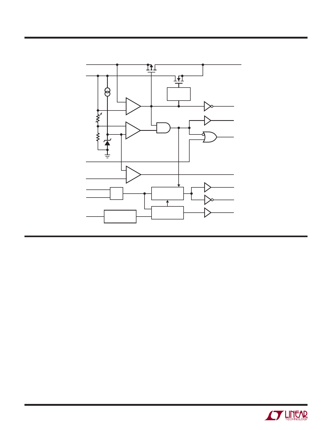
BLOCK DIAGRAM
VBATT
VCC
CE IN
PFI
OSC IN
OSC SEL
WDI
–
C2
+
+
C1
–
1.3V
GND
–
C3
+
OSC
TRANSITION
DETECTOR
M2
M1
CHARGE
PUMP
RESET PULSE
GENERATOR
WATCHDOG
TIMER
VOUT
BATT ON
LOW⎯LINE
CE OUT
PFO
RESET
RESET
WDO
690 BD
PIN FUNCTIONS
VCC: 5V Supply Input. The VCC pin should be bypassed
with a 0.1μF capacitor.
VOUT: Voltage Output for Backed Up Memory. Bypass with
a capacitor of 0.1μF or greater. During normal operation,
VOUT obtains power from VCC through an NMOS power
switch, M1, which can deliver up to 50mA and has a typical
on resistance of 5Ω. When VCC is lower than VBATT, VOUT
is internally switched to VBATT. If VOUT and VBATT are not
used, connect VOUT to VCC.
VBATT: Back-Up Battery Input. When VCC falls below VBATT,
auxiliary power, connected to VBATT, is delivered to VOUT
through PMOS switch, M2. If back-up battery or auxiliary
power is not used, VBATT should be connected to GND.
GND: Ground pin.
BATT ON: Battery On Logic Output from Comparator C2.
BATT ON goes low when VOUT is internally connected to
VCC. The output typically sinks 35mA and can provide
base drive for an external PNP transistor to increase the
output current above the 50mA rating of VOUT. BATT ON
goes high when VOUT is internally switched to VBATT.
PFI: Power Failure Input. PFI is the noninverting input
to the power-fail comparator, C3. The inverting input is
internally connected to a 1.3V reference. The power failure
output remains high when PFI is above 1.3V and goes
low when PFI is below 1.3V. Connect PFI to GND or VOUT
when C3 is not used.
690fe
6
Share Link: 