LTC5564IUDPBF Просмотр технического описания (PDF) - Linear Technology
Номер в каталоге
Компоненты Описание
производитель
LTC5564IUDPBF Datasheet PDF : 16 Pages
| |||
LTC5564
APPLICATIONS INFORMATION
Operation
The LTC5564 is a fast RF detector with a high speed
amplifier and comparator. This product integrates these
functions to provide RF detection over frequencies ranging
from 600MHz to 15GHz. These functions include an RF
Schottky peak detector, internally compensated operational
amplifier, and a comparator as shown in Figure 1. The
LTC5564 has selectable amplifier gains, amplifier output
offset adjustment and comparator latch enable capabilities.
Amplifier
The high speed amplifier offers four gain settings and
is capable of driving a 1.7mA load with an output swing
range of approximately 295mV to VCC – 1.6V. See Table 1
for gain setting operation.
The VOUTADJ pin provides output DC offset adjustment
to satisfy various interface requirements. Setting VOUT
to 500mV also provides the maximum demodulation
bandwidth in each gain mode. See Electrical and Typical
Performance Characteristics curve. See Table 1 for the
typical VOUTADJ voltage for the desired VOUT DC output
offset in each gain setting.
RF Detector
The internal temperature compensated Schottky diode
peak detector converts the RF input signal to a low
frequency signal. The detector demonstrates excellent
efficiency and linearity over a wide range of input power
levels. The Schottky diode is nominally biased at 180µA
and drives a parallel reservoir capacitor-resistor network
of 8pF and 1.2k.
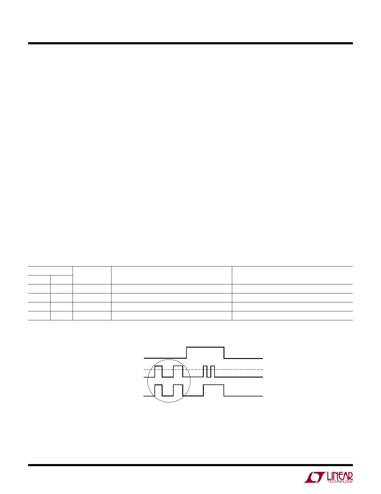
Comparator
The high speed comparator compares the external refer-
ence voltage on the VREF pin to the internal signal voltage
VP from the peak detector and produces the output logic
signal VCOMP . VP is the internal comparator positive input
as shown in Figure 1.
LEN provides latch enable/disable functionality as shown
in Figure 2.
Table 1. Gain Mode and Typical VOUTADJ Operation
PIN
G1
G0
GAIN MODE DESCRIPTION
GND GND
GAIN1
Minimum Gain Setting (VOUT/RFIN ≈ 1.5dB)
GND
VCCA
GAIN2
VOUT/RFIN Increased 6dB
VCCA
GND
GAIN4
VOUT/RFIN Increased 12dB
VCCA
VCCA
GAIN8
VOUT/RFIN Increased 18dB
Note: Valid range for VOUT ≈ 0.195V ≤ VOUT ≤ VCC – 1.6
REQUIRED VOUTADJ FOR A GIVEN DC OUTPUT OFFSET
VOUTADJ = 0.95 • VOUT – 0.174
VOUTADJ = (VOUT – 0.07)/2.10
VOUTADJ = (VOUT + 0.05)/3.16
VOUTADJ = (VOUT + 0.25)/5.26
LEN
VREF
VP
VCOMP
VOUT
TRANSPARENT
VOUT
LATCHED
5564 F02
VOUT
TRANSPARENT
Figure 2. LTC5564 Comparator Latch Enable Function
5564fc
10
For more information www.linear.com/LTC5564
Share Link: 