LTC4101 Просмотр технического описания (PDF) - Linear Technology
Номер в каталоге
Компоненты Описание
производитель
LTC4101 Datasheet PDF : 30 Pages
| |||
LTC4101
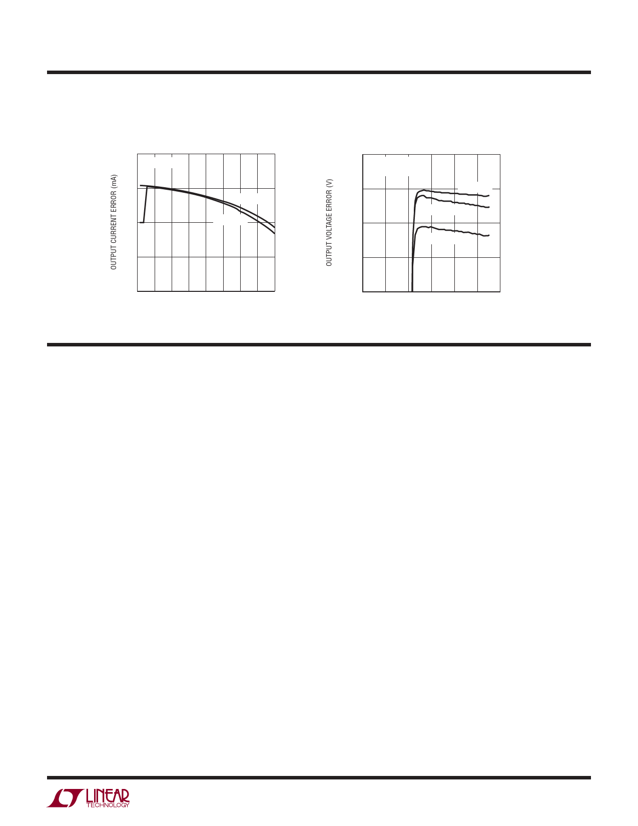
TYPICAL PERFORMANCE CHARACTERISTICS TA = 25°C, unless otherwise noted.
Charging Current Error
200
VDD = 5V
100
VDCIN = 20V
0
VDCIN = 9V
–100
–200
0
1
2
3
CHARGING CURRENT (A)
4
4101 G09
Transfer Function of Charger
50
VDD = 5V
IBAT = 0.120A
0
VDCIN = 9V
–50
–100
VDCIN = 20V
VDCIN = 28V
–150
0
1
2
34
5
6
CHARGING VOLTAGE (V)
4101 G10
PIN FUNCTIONS
TGATE (Pin 1): Drives the Top External P-MOSFET of the
Battery Charger Buck Converter.
PGND (Pin 2): High Current Ground Return for BGATE
Driver.
BGATE (Pin 3): Drives the Bottom External N-MOSFET of
the Battery Charger Buck Converter.
INFET (Pin 4): Drives the Gate of the External Input
P-MOSFET.
DCIN (Pin 5): External DC Power Source Input. Bypass to
ground with a 0.1μF capacitor.
CHGEN (Pin 6): Digital Bidirectional Pin to Enable Charger
Function. This pin is connected as a wired AND bus.
The following events will cause the POWER_FAIL bit in
the ChargerStatus register to become set:
1. An external device pulling the CHGEN signal to within
0.9V to GND;
2. The AC adapter voltage is not above the battery
voltage.
SMBALERT (Pin 7): Active Low Interrupt Output to Host
(referred to as the SMBALERT signal in the SMBus Revi-
sion 1.1 specification). Signals host that there has been a
change of status in the charger registers and that the host
should read the LTC4101 status registers to determine
if any action on its part is required. This signal can be
connected to the optional SMBALERT line of the SMBus.
Open drain with weak current source pull-up to VDD (with
Schottky to allow it to be pulled to 5V externally).
SDA (Pin 8): SMBus Data Signal from Main (host-con-
trolled) SMBus. External pull-up resistor is required.
SCL (Pin 9): SMBus Clock Signal from Main (host-con-
trolled) SMBus. External pull-up resistor is required.
ACP (Pin 10): This Output Indicates the Value of the
DCDIV Comparator. It can be used to indicate whether
AC is present or not.
DCDIV (Pin 11): Supply Divider Input. This is a high im-
pedance comparator input with a 1.2V threshold (rising
edge) and hysteresis.
GND (Pin 12): Ground for Digital and Analog Circuitry.
4101fa
7
Share Link: 