LTC4101 Просмотр технического описания (PDF) - Linear Technology
Номер в каталоге
Компоненты Описание
производитель
LTC4101 Datasheet PDF : 30 Pages
| |||
LTC4101
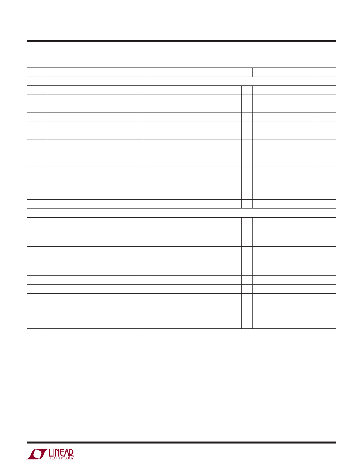
ELECTRICAL CHARACTERISTICS The l denotes the specifications which apply over the full operating
temperature range, otherwise specifications are at TA = 25°C. VDCIN = 20V, VDD = 3.3V, VBAT = 4V unless otherwise noted. (Note 4)
SYMBOL PARAMETER
CONDITIONS
MIN
TYP
MAX UNITS
Logic Levels
VIL
SCL/SDA Input Low Voltage
VDD = 3V and VDD = 5.5V
l
0.8
V
VIH
SCL/SDA Input High Voltage
VDD = 3V and VDD = 5.5V
l 2.1
V
VOL
SDA Output Low Voltage
IPULL-UP = 350μA
l
0.4
V
IIL
SCL/SDA Input Current
VSDA, VSCL = VIL
–1
1
μA
IIH
SCL/SDA Input Current
VSDA, VSCL = VIH
–1
1
μA
VOL
SMBALERT Output Low Voltage
IPULL-UP = 500μA
l
0.4
V
SMBALERT Output Pull-Up Current
VSMBALERT = VOL
–17.5 –10
–3.5
μA
ILEAK
SDA/SCL/SMBALERT Power Down Leakage VSDA, VSCL, VSMBALERT = 5.5V, VDD = OV
l –2
2
μA
VOL
CHGEN Output Low Voltage
IOL = 100μA
l
0.5
V
CHGEN Output Pull-Up Current
VCHGEN = VOL
–17.5 –10
–3.5
μA
VIL
CHGEN Input Low Voltage
l
0.9
V
VIH
CHGEN Input High Voltage
VDD = 3V
VDD = 5.5V
l 2.5
V
3.9
V
Power-On Reset Duration
VDD Ramp from 0V to >3V in <5μs
100
μs
SMBus Timing (Refer to System Management Bus Specification, Revision 1.1, Section 2.1 for Timing Diagrams)
tHIGH SCL Serial Clock High Period
tLOW
SCL Serial Clock Low Period
tR
SDA/SCL Rise Time
tF
SDA/SCL Fall Time
tSU:STA
tHD:STA
tHD:DAT
Start Condition Setup Time
Start Condition Hold Time
SDA to SCL Falling-Edge Hold Time,
Slave Clocking in Data
IPULL-UP = 350μA, CLOAD = 250pF, RPU = 9.31k, l
4
VDD = 3V and VDD = 5.5V
IPULL-UP = 350μA, CLOAD = 250pF, RPU = 9.31k, l 4.7
VDD = 3V and VDD = 5.5V
CLOAD = 250pF, RPU = 9.31k, VDD = 3V
l
and VDD = 5.5V
CLOAD = 250pF, RPU = 9.31k, VDD = 3V
l
and VDD = 5.5V
VDD = 3V and VDD = 5.5V
l 4.7
VDD = 3V and VDD = 5.5V
l4
VDD = 3V and VDD = 5.5V
l 300
μs
15000
μs
1000
ns
300
ns
μs
μs
ns
tTIMEOUT Time Between Receiving Valid
ChargingCurrent() and
ChargingVoltage() Commands
VDD = 3V and VDD = 5.5V
l 140
175
210
sec
Note 1: Stresses beyond those listed under Absolute Maximum Ratings
may cause permanent damage to the device. Exposure to any Absolute
Maximum Rating condition for extended periods may affect device
reliability and lifetime.
Note 2: See Test Circuit.
Note 3: Does not include tolerance of current sense resistor.
Note 4: The LTC4101E is guaranteed to meet performance specifications
from 0°C to 85°C. Specifications over the –40°C to 85°C operating
temperature range are assured by design, characterization and correlation
with statistical process controls.
Note 5: Current accuracy dependent upon circuit compensation and sense
resistor.
Note 6: CTH is defined as the sum of capacitance on THA, THB and
SafetySignal.
Note 7: The corresponding overrange bit will be set when a HEX value
greater than or equal to this value is used.
4101fa
5
Share Link: 