LTC3418 Просмотр технического описания (PDF) - Linear Technology
Номер в каталоге
Компоненты Описание
производитель
LTC3418 Datasheet PDF : 20 Pages
| |||
LTC3418
ELECTRICAL CHARACTERISTICS The l denotes the specifications which apply over the full operating
temperature range, otherwise specifications are at TA = 25°C. VIN = 3.3V. (Note 2)
SYMBOL
ITRACK
ΔVPGOOD
RPGOOD
IQ
fOSC
fSYNC
RPFET
RNFET
ILIMIT
VUVLO
VREF
ILSW
VRUN
PARAMETER
TRACK Input Current
Power Good Range
Power Good Resistance
Input DC Bias Current
Active Current
Shutdown
Switching Frequency
Switching Frequency Range
SYNC Capture Range
RDS(ON) of P-Channel FET
RDS(ON) of N-Channel FET
Peak Current Limit
Undervoltage Lockout Threshold
Reference Output
SW Leakage Current
RUN Threshold
CONDITIONS
(Note 4)
VFB = 0.7V, VITH = 1V
VRUN = 0V
ROSC = 69.8kΩ
(Note 6)
(Note 6)
ISW = 600mA
ISW = – 600mA
VRUN = 0V, VIN = 5.5V
MIN TYP MAX UNITS
100 200
nA
±7.5
±9
%
100
150
Ω
380 450
μA
0.03 1.5
μA
0.88
1
1.12
MHz
0.3
4
MHz
0.3
4
MHz
35
50
mΩ
25
35
mΩ
12
17
A
1.75
2
2.25
V
1.219 1.250 1.281
V
0.1
1
μA
0.5
0.65
0.8
V
Note 1: Stresses beyond those listed under Absolute Maximum Ratings
may cause permanent damage to the device. Exposure to any Absolute
Maximum Rating condition for extended periods may affect device
reliability and lifetime.
Note 2: The LTC3418 is guaranteed to meet performance specifications
from 0°C to 85°C. Specifications over the –40°C to 85°C operating
temperature range are assured by design, characterization and
correlation with statistical process controls.
Note 3: The LTC3418 is tested in a feedback loop that adjusts VFB to
achieve a specified error amplifier output voltage (ITH).
Note 4: Dynamic supply current is higher due to the internal gate charge
being delivered at the switching frequency.
Note 5: TJ is calculated from the ambient temperature TA and power
dissipation PD as follows:
LTC3418: TJ = TA + (PD)(34°C/W)
Note 6: This parameter is guaranteed by design and characterization.
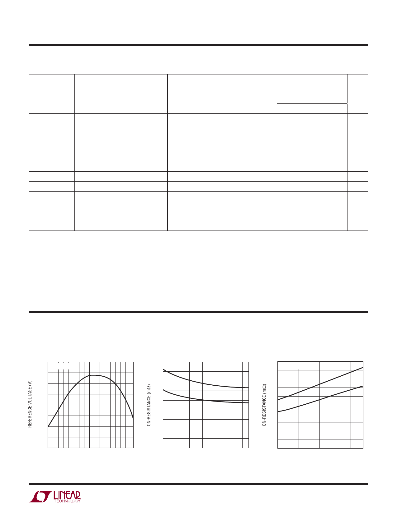
TYPICAL PERFORMANCE CHARACTERISTICS TA = 25°C unless otherwise noted.
Internal Reference Voltage
vs Temperature
0.8000 VIN = 3.3V
0.7995
0.7990
0.7985
0.7980
0.7975
0.7970
0.7965
0.7960
–40 –20
0 20 40 60 80 100 120
TEMPERATURE (°C)
3418 G01
Switch On-Resistance
vs Input Voltage
45
40
35
PFET
30
NFET
25
20
15
10
5
0
2.25 2.75 3.25 3.75 4.25 4.75 5.25
INPUT VOLTAGE (V)
3418 G02
On-Resistance vs Temperature
50
VIN = 3.3V
45
40
PFET
35
30
NFET
25
20
15
10
5
0
–40 –20 0 20 40 60 80 100 120
TEMPERATURE (°C)
3418 G03
3418fb
3
Share Link: 