LTC2902 Просмотр технического описания (PDF) - Linear Technology
Номер в каталоге
Компоненты Описание
производитель
LTC2902
Linear Technology

LTC2902 Datasheet PDF : 16 Pages
| |||
LTC2902
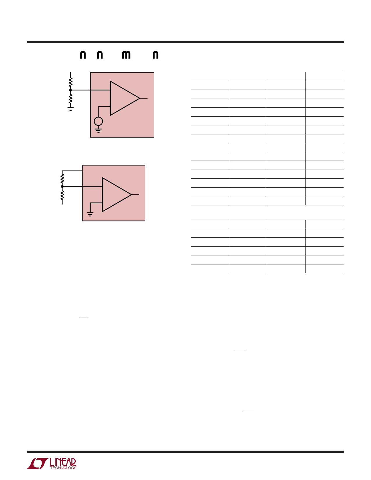
APPLICATIO S I FOR ATIO
VTRIP
R3
1%
V3 OR V4
R4
1%
LTC2902
+
–
+–
0.5V
5% TOLERANCE MODE
2902 F05
Figure 5. Setting the Positive Adjustable Trip Point
12
VREF
R4
1% 13 V4
R3
1%
VTRIP
LTC2902
–
+
2902 F06
Figure 6. Setting the Negative Adjustable Trip Point
In the negative adjustable mode, the noninverting input on
the V4 comparator is connected to ground (Figure 6). The
tap point on an external resistive divider, connected be-
tween the negative voltage being sensed and the VREF pin,
is connected to the high impedance inverting input (V4).
VREF provides the necessary level shift required to operate
at ground. The trip voltage is calculated from:
VTRIP
=
–
VREF
R3
R4
;
VREF
=
1.210V
T0,T1 Low (5% Tolerance Mode)
Once the resistor divider is set in the 5% tolerance mode,
there is no need to change the divider for the other
tolerance modes (7.5%, 10%, 12.5%) because VREF is
scaled accordingly, moving the trip point in – 2.5%
increments.
In a negative adjustable application, the minimum value
for R4 is limited by the sourcing capability of VREF (±1mA).
With no other load on VREF, R4 (minimum) is:
1.21V ÷ 1mA = 1.21kΩ
Tables 2 and 3 offer suggested 1% resistor values for
various adjustable applications.
Table 2. Suggested 1% Resistor Values for the ADJ Inputs
VSUPPLY (V)
12
VTRIP (V)
11.25
R3 (kΩ)
2150
R4 (kΩ)
100
10
9.4
1780
100
8
7.5
1400
100
7.5
7
1300
100
6
5.6
1020
100
5
4.725
845
100
3.3
3.055
511
100
3
2.82
464
100
2.5
2.325
365
100
1.8
1.685
237
100
1.5
1.410
182
100
1.2
1.120
124
100
1
0.933
86.6
100
0.9
0.840
68.1
100
Table 3. Suggested 1% Resistor Values for the –ADJ Input
VSUPPLY (V)
–2
VTRIP (V)
–1.87
R3 (kΩ)
187
R4 (kΩ)
121
–5
– 4.64
464
121
– 5.2
– 4.87
487
121
–10
– 9.31
931
121
–12
–11.30
1130
121
Although all four supply monitor comparators have built-in
glitch immunity, bypass capacitors on V1 and V2 are
recommended because the greater of V1 or V2 is also the
VCC for the chip. Filter capacitors on the V3 and V4 inputs
are allowed.
Power-Down
On power-down, once any of the VX inputs drop below
their threshold, RST and COMPX are held at a logic low.
A logic low of 0.4V is guaranteed until both V1 and V2
drop below 1V. If the bandgap reference becomes invalid
(VCC < 2V typ), the part will reprogram once VCC rises
above 2.4V (max).
Monitor Output Rise and Fall Time Estimation
All of the outputs (RST, COMPX) have strong pull-down
capability. If the external load capacitance (CLOAD) for a
2902f
11
Share Link: