LTC2902 Просмотр технического описания (PDF) - Linear Technology
Номер в каталоге
Компоненты Описание
производитель
LTC2902
Linear Technology

LTC2902 Datasheet PDF : 16 Pages
| |||
LTC2902
APPLICATIO S I FOR ATIO
Power-Up
On power-up, the larger of V1 or V2 will power the drive
circuits for the RST and the COMPX pins. This ensures
that the RST and COMPX outputs will be low as soon as
V1 or V2 reaches 1V. The RST and COMPX outputs will
remain low until the part is programmed. After program-
ming, if any one of the VX inputs is below its programmed
threshold, RST will be a logic low. Once all the VX inputs
rise above their thresholds, an internal timer is started
and RST is released after the programmed delay time. If
VCC < (V3 – 1) and VCC < 2.4V, the V3 input impedance
will be low (1kΩ typ).
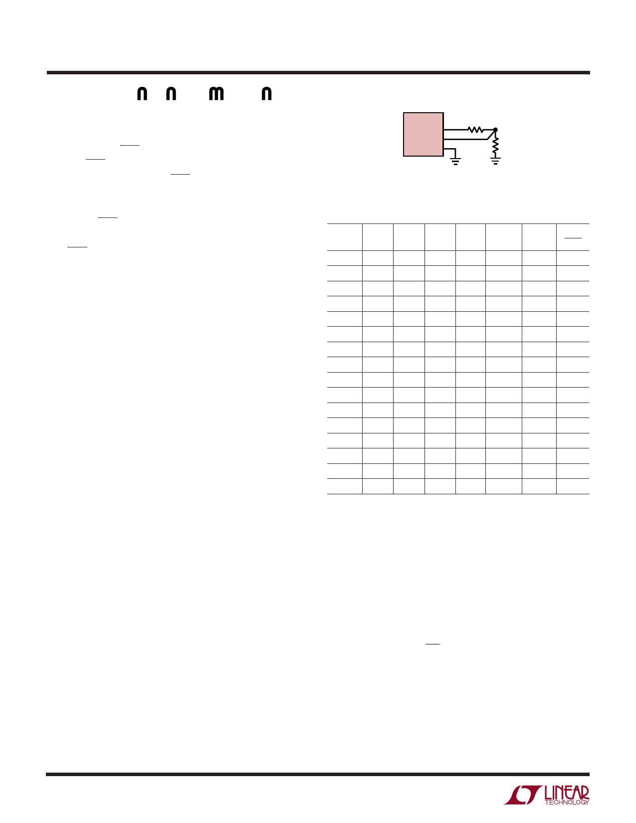
Monitor Programming
The LTC2902 input voltage combination is selected by
placing the recommended resistor divider from VREF to
GND and connecting the tap point to VPG, as shown in
Figure 4. Table 1 offers recommended 1% resistor values
for the various modes. The last column in Table 1 speci-
fies optimum VPG/VREF ratios (±0.01) to be used when
programming with a ratiometric DAC.
During power-up, once V1 or V2 reaches 2.4V (max), the
monitor enters a programming period of approximately
150µs during which the voltage on the VPG pin is sampled
and the monitor is configured to the desired input combi-
nation. Do not add capacitance to the VPG pin. Immediately
after programming, the comparators are enabled and
supply monitoring will begin.
Supply Monitoring
The LTC2902 is a low power, high accuracy program-
mable quad supply monitoring circuit with four nondelayed
monitor outputs, a common reset output and selectable
supply thresholds. Reset timing is adjustable using an
external capacitor. Single pin programming selects 1 of 16
input voltage monitor combinations. Two digital inputs
select one of four supply tolerances (5%, 7.5%, 10% or
12.5%). All four voltage inputs must be above predeter-
mined thresholds for the reset not to be invoked. The
LTC2902 will assert the reset and comparator outputs
during power-up, power-down and brownout conditions
on any one of the voltage inputs.
R1
LTC2902
VREF
VPG
GND
12
11
10
1%
R2
1%
2902 F04
Figure 4. Monitor Programming
Table 1. Voltage Threshold Programming
VPG
MODE V1 (V) V2 (V) V3 (V) V4 (V) R1 (kΩ) R2 (kΩ) VREF
0
5.0 3.3 ADJ ADJ Open Short 0.000
1
5.0 3.3 ADJ –ADJ 93.1 9.53 0.094
2
3.3 2.5 ADJ ADJ 86.6 16.2 0.156
3
3.3 2.5 ADJ –ADJ 78.7 22.1 0.219
4
3.3 2.5 1.5 ADJ 71.5 28.0 0.281
5
5.0 3.3 2.5 ADJ 66.5 34.8 0.344
6
5.0 3.3 2.5 1.8 59.0 40.2 0.406
7
5.0 3.3 2.5 1.5 53.6 47.5 0.469
8
5.0 3.0 2.5 ADJ 47.5 53.6 0.531
9
5.0 3.0 ADJ ADJ 40.2 59.0 0.594
10 3.3 2.5 1.8 1.5 34.8 66.5 0.656
11 3.3 2.5 1.8 ADJ 28.0 71.5 0.719
12 3.3 2.5 1.8 –ADJ 22.1 78.7 0.781
13 5.0 3.3 1.8 –ADJ 16.2 86.6 0.844
14 5.0 3.3 1.8 ADJ 9.53 93.1 0.906
15 5.0 3.0 1.8 ADJ Short Open 1.000
The inverting inputs on the V3 and/or V4 comparators are
set to 0.5V when the positive adjustable modes are selected
and with T0 and T1 low (5% tolerance) (Figure 5). The tap
point on an external resistive divider, connected between
the positive voltage being sensed and ground, is connected
to the high impedance noninverting inputs (V3, V4). The
trip voltage is calculated from:
VTRIP = 0.5V1+ RR34
Once the resistor divider is set in the 5% tolerance mode,
there is no need to change the divider for the other
tolerance modes (7.5%, 10%, 12.5%) because the inter-
nal reference is scaled accordingly, moving the trip point
in – 2.5% increments.
2902f
10
Share Link: