LTC2901-2IGN Просмотр технического описания (PDF) - Linear Technology
Номер в каталоге
Компоненты Описание
производитель
LTC2901-2IGN
Linear Technology

LTC2901-2IGN Datasheet PDF : 16 Pages
| |||
LTC2901
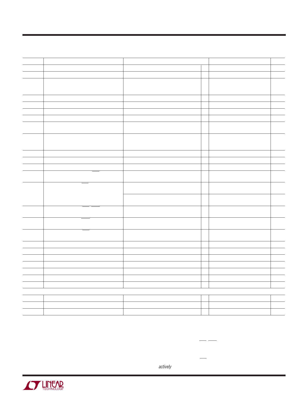
ELECTRICAL CHARACTERISTICS The ● denotes the specifications which apply over the full operating
temperature range, otherwise specifications are at TA = 25°C. VCC = 5V, unless otherwise noted. (Notes 3, 4)
SYMBOL PARAMETER
CONDITIONS
MIN TYP MAX
VCCMINP
VCCMINC
VREF
Minimum Required for Programming
Minimum Required for Comparators
Reference Voltage
VPG
Programming Voltage Range
IVPG
VPG Input Current
IV1
V1 Input Current
IV2
V2 Input Current
IV3
V3 Input Current
VCC Rising
●
VCC Falling
●
VCC ≥ 2.3V, IVREF = ±1mA, CREF ≤ 1000pF
T0L Low
●
T0L High
●
VCC ≥ VCCMINP
●
VPG = VREF
●
V1 = 5V, IVREF = 12µA, (Note 5)
●
V2 = 3.3V
●
V3 = 2.5V
●
V3 = 0.55V (ADJ Mode)
●
2.42
2.32
1.192
1.128
0
–15
1.210
1.146
43
0.8
0.52
1.228
1.163
VREF
±20
75
2
1.2
15
IV4
V4 Input Current
V4 = 1.8V
V4 = 0.55V (ADJ Mode)
V4 = –0.05V (–ADJ Mode)
●
0.34
0.8
●
–15
15
●
–15
15
ICRT(UP)
ICRT(DN)
tRST
tUV
CRT Pull-Up Current
CRT Pull-Down Current
Reset Time-Out Period
VX Undervoltage Detect to RST or COMPX
VCRT = 0V
VCRT = 1.3V
CRT = 1500pF
VX Less Than Reset Threshold VRTX
by More Than 1%
●
– 1.4
–2
– 2.6
●
10
20
30
●
5
7
9
150
VOL
Output Voltage Low RST, COMPX
ISINK = 2.5mA; V1 = 3V, V2 = 3V;
●
V3, V4 = 0V; VPG = 0V
0.15
0.4
ISINK = 100µA; V2 = 1V; V1, V3, V4 = 0V ●
ISINK = 100µA; V1 = 1V; V2, V3, V4 = 0V ●
0.05
0.3
0.05
0.3
VOH
Output Voltage High RST, WDO, COMPX ISOURCE = 1µA
(Note 6)
● V2 – 1
VOL
Output Voltage Low WDO
VOH
Output Voltage High RST
(LTC2901-2/LTC2901-4) (Note 7)
ISINK = 2.5mA; V1 = 5V, V2 = 3.3V;
V3, V4 = 1V; VPG = 0V
ISOURCE = 200µA
●
0.15
0.4
● 0.8 • V2
ICWT(UP) CWT Pull-Up Current
ICWT(DN) CWT Pull-Down Current
tWD
Watchdog Time-Out Period
VIH
WDI Input Threshold High
VIL
WDI Input Threshold Low
tWP
WDI Input Pulse Width
IWDI
WDI Pull-Up Current
Digital Input T0L
VCWT = 0V
VCWT = 1.3V
CWT = 1500pF
VCC = 3.3V to 5.5V
VCC = 3.3V to 5.5V
VCC = 3.3V
VWDI = 0V
●
– 1.4
–2
– 2.6
●
10
20
30
●
20
30
40
●
1.6
●
0.4
●
150
– 10
VIL
VIH
IINTOL
T0L Low Level Input Voltage
T0L High Level Input Voltage
T0L Input Current
VCC = 3.3V to 5.5V
VCC = 3.3V to 5.5V
TOL = VCC
●
0.3VCC
● 0.7VCC
●
±0.1
±1
UNITS
V
V
V
V
V
nA
µA
µA
µA
nA
µA
nA
nA
µA
µA
ms
µs
V
V
V
V
V
V
µA
µA
ms
V
V
ns
µA
V
V
µA
Note 1: Stresses beyond those listed under Absolute Maximum Ratings may
cause permanent damage to the device. Exposure to any Absolute Maximum
Rating condition for extended periods may affect device reliability and
lifetime.
Note 2: All currents into pins are positive, all voltages are referenced to GND
unless otherwise noted.
Note 3: The greater of V1, V2 is the internal supply voltage (VCC).
Note 4: 10% thresholds apply to the LTC2901-3/LTC2901-4 only when the
TOL pin is set to a logic high.
Note 5: Under static no-fault conditions, V1 will necessarily supply quiescent
current. If at any time V2 is larger than V1, V2 must be capable of supplying
the quiescent current, programming (transient) current and reference load
current.
Note 6: The output pins RST, WDO and COMPX have internal pull-ups to V2
of typically 6µA. However, external pull-up resistors may be used when faster
rise times are required or for VOH voltages greater than V2.
Note 7: The push-pull RST output pin on the LTC2901-2/LTC2901-4 is
actively pulled up to V2.
2901fb
3
Downloaded from: http://www.datasheetcatalog.com/
Share Link: