LTC2208IUP-14 Просмотр технического описания (PDF) - Linear Technology
Номер в каталоге
Компоненты Описание
производитель
LTC2208IUP-14 Datasheet PDF : 28 Pages
| |||
LTC2208-14
ELECTRICAL CHARACTERISTICS
Note 1: Stresses beyond those listed under Absolute Maximum Ratings
may cause permanent damage to the device. Exposure to any Absolute
Maximum Rating condition for extended periods may affect device
reliability and lifetime.
Note 2: All voltage values are with respect to GND, with GND and OGND
shorted (unless otherwise noted).
Note 3: When these pin voltages are taken below GND or above VDD, they
will be clamped by internal diodes. This product can handle input currents
of greater than 100mA below GND or above VDD without latchup.
Note 4: VDD = 3.3V, fSAMPLE = 130MHz, LVDS outputs, differential ENC+/
ENC– = 2VP-P sine wave with 1.6V common mode, input range = 2.25VP-P
with differential drive (PGA = 0), unless otherwise specified.
Note 5: Integral nonlinearity is defined as the deviation of a code from a “best
fit straight line” to the transfer curve. The deviation is measured from the
center of the quantization band.
Note 6: Offset error is the offset voltage measured from –1/2LSB when the
output code flickers between 00 0000 0000 0000 and 11 1111 1111 1111 in
2’s complement output mode.
Note 7: Guaranteed by design, not subject to test.
Note 8: Recommended operating conditions.
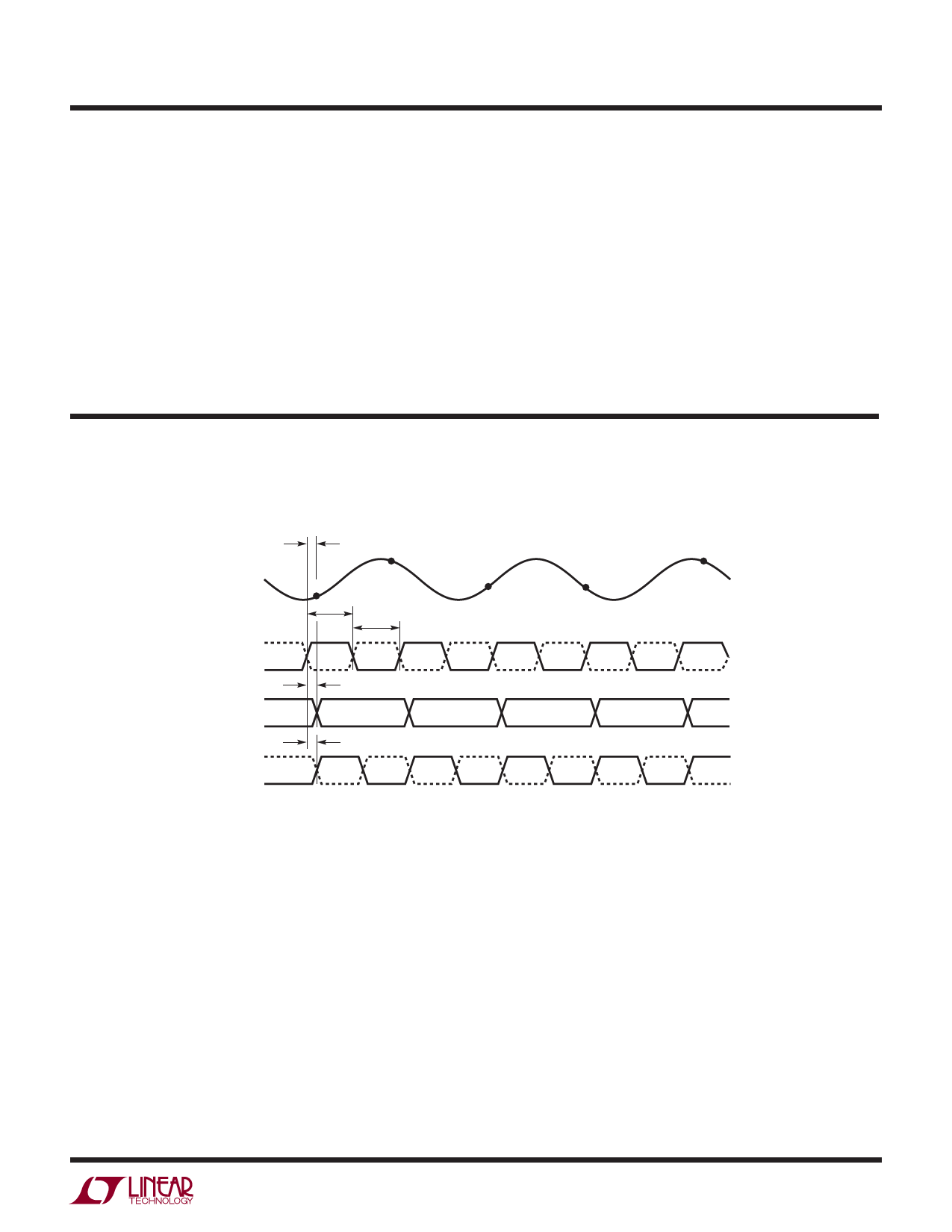
TIMING DIAGRAM
LVDS Output Mode Timing
All Outputs are Differential and Have LVDS Levels
ANALOG
INPUT
ENC–
ENC+
D0-D13, OF
CLKOUT+
CLKOUT –
tAP
N+1
N
tH
tL
N+2
N+3
tD
N–7
tC
N–6
N–5
N–4
N+4
N–3
220814 TD01
220814fb
7
Share Link: 