LTC1272-3ACS –ü—Ä–æ—Å–º–æ—Ç—Ä —Ç–µ—Ö–Ω–∏—á–µ—Å–∫–æ–≥–æ –æ–ø–∏—Å–∞–Ω–∏—è (PDF) - Linear Technology
–ù–æ–º–µ—Ä –≤ –∫–∞—Ç–∞–ª–æ–≥–µ
–ö–æ–º–ø–æ–Ω–µ–Ω—Ç—ã –û–ø–∏—Å–∞–Ω–∏–µ
–ø—Ä–æ–∏–∑–≤–æ–¥–∏—Ç–µ–ª—å
LTC1272-3ACS Datasheet PDF : 20 Pages
| |||
LTC1272
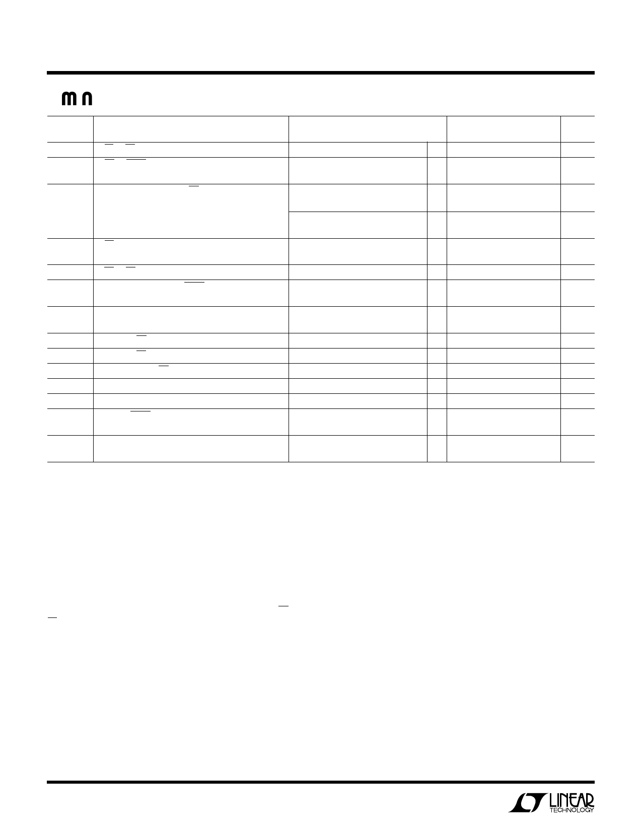
TI I G CHARACTERISTICS (Note 8)
SYMBOL
t1
t2
t3
PARAMETER
CS to RD Setup Time
RD to BUSY Delay
Data Access Time After RD‚Üì
t4
t5
t6
t7
t8
t9
t10
t11
t12
t13
tCONV
RD Pulse Width
CS to RD Hold Time
Data Setup Time After BUSY
Bus Relinquish Time
HBEN to RD Setup Time
HBEN to RD Hold Time
Delay Between RD Operations
Delay Between Conversions
Aperture Delay of Sample and Hold
CLK to BUSY Delay
Conversion Time
CONDITIONS
CL = 50pF
COM Grade
CL = 20pF
COM Grade
CL = 100pF
COM Grade
COM Grade
COM Grade
COM Grade
Jitter < 50ps
COM Grade
LTC1272-XA/C
MIN TYP MAX
UNITS
q
0
ns
80
190
ns
q
230
ns
50
90
ns
q
110
ns
70
125
ns
q
150
ns
t3
ns
q
t3
ns
q
0
ns
40
70
ns
q
90
ns
20
30
75
ns
q 20
85
ns
q
0
ns
q
0
ns
q 200
ns
1
µs
25
ns
80
170
ns
q
220
ns
q 12
13
CLK
CYCLES
The q indicates specifications which apply over the full operating
temperature range; all other limits and typicals TA = 25°C.
Note 1: Absolute maximum ratings are those values beyond which the life
of a device may be impaired.
Note 2: All voltage values are with respect to ground with DGND and
AGND wired together, unless otherwise noted.
Note 3: When the analog input voltage is taken below ground it will be
clamped by an internal diode. This product can handle, with no external
diode, input currents of greater than 60mA below ground without latch-up.
Note 4: VDD = 5V, fCLK = 4MHz for LTC1272-3, and 1.6MHz for
LTC1272-8, tr = tf = 5ns unless otherwise specified. For best analog
performance, the LTC1272 clock should be synchronized to the RD and
CS control inputs with at least 40ns separating convert start from the
nearest clock edge.
Note 5: Linearity error is specified between the actual end points of the
A/D transfer curve.
Note 6: The LTC1272 has the same 0V to 5V input range as the AD7572
but, to achieve single supply operation, it provides a 2.42V reference
output instead of the –5.25V of the AD7572. This requires that the polarity
of the reference bypass capacitor be reversed when plugging an LTC1272
into an AD7572 socket.
Note 7: Guaranteed by design, not subject to test.
Note 8: VDD = 5V. Timing specifications are sample tested at 25°C to
ensure compliance. All input control signals are specified with tr = tf = 5ns
(10% to 90% of 5V) and timed from a voltage level of 1.6V. See Figures 13
through 17.
4
Share Link: 