LCX020 Просмотр технического описания (PDF) - Sony Semiconductor
Номер в каталоге
Компоненты Описание
производитель
LCX020 Datasheet PDF : 24 Pages
| |||
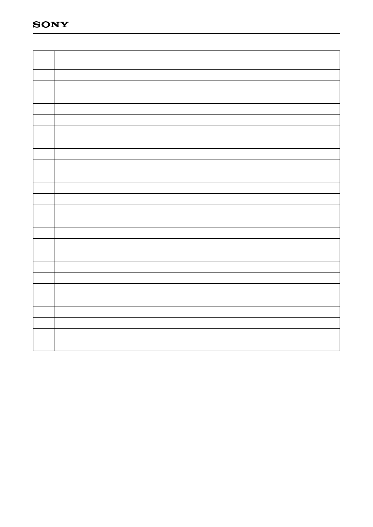
Pin
No.
Symbol
Description
15 SIGG5 Video signal input to panel (G-5)
16 SIGG6 Video signal input to panel (G-6)
17 SIGB1 Video signal input to panel (B-1)
18 SIGB2 Video signal input to panel (B-2)
19 SIGB3 Video signal input to panel (B-3)
20 SIGB4 Video signal input to panel (B-4)
21 SIGB5 Video signal input to panel (B-5)
22 SIGB6 Video signal input to panel (B-6)
23 HVDD
Power supply input for H driver
24 RGT
Drive direction input for H shift register (H: normal, L: reverse)
25 MODE3 Display area switching 3 input
26 MODE2 Display area switching 2 input
27 MODE1 Display area switching 1 input
28 HST
Start pulse input for H shift register drive
29 HCK1 Clock pulse input for H shift register drive
30 HCK2 Clock pulse input for H shift register drive
31 VSS
GND (H, V drivers)
32 BLK
Black frame display pulse input
33 ENB
Gate selection pulse enable input
34 VCK
Clock pulse input for V shift register drive
35 VST
Start pulse input for V shift register drive
36 DWN
Drive direction input for V shift register (H: normal, L: reverse)
37 PCG
Uniformity improvement pulse input
38 VVDD
Power supply input for V driver
39 SOUT H and V shift register drive checking (Test pin; no connection.)
LCX020BK
–4–
Share Link: 