LTC1044A Просмотр технического описания (PDF) - Linear Technology
Номер в каталоге
Компоненты Описание
производитель
LTC1044A Datasheet PDF : 14 Pages
| |||
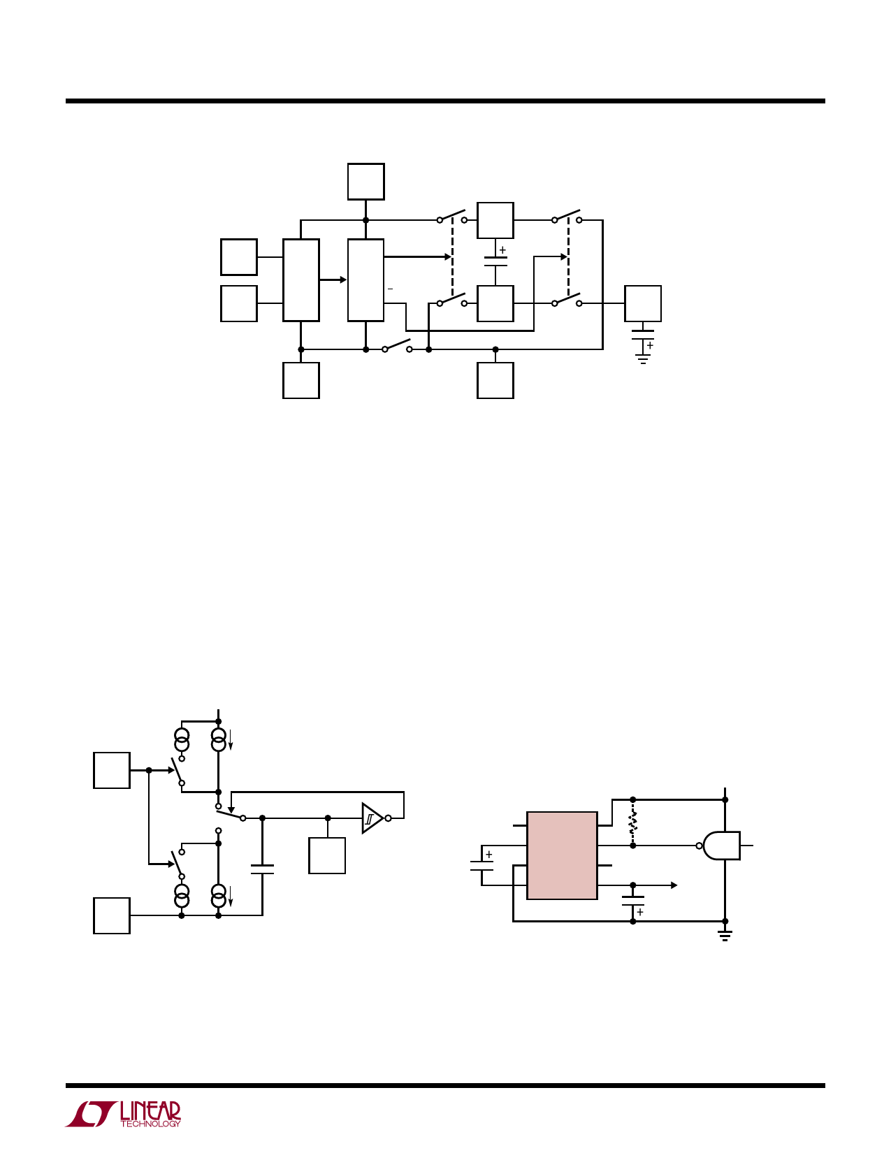
LTC1044A
Applications Information
BOOST
7X
(1)
OSC
OSC
(7)
LV
(6)
V+
(8)
φ
÷2
φ
SW1
C+
(2)
C1
C–
(4)
CLOSED WHEN
V+ > 3V
GND
(3)
SW2
1044a F03
VOUT
(5)
C2
Figure 3. LTC1044A Switched-Capacitor Voltage Converter Block Diagram
LV (Pin 6)
The internal logic of the LTC1044A runs between V+ and
LV (pin 6). For V+ greater than or equal to 3V, an internal
switch shorts LV to GND (pin 3). For V+ less than 3V, the
LV pin should be tied to GND. For V+ greater than or equal
to 3V, the LV pin can be tied to GND or left floating.
OSC (Pin 7) and Boost (Pin 1)
The switching frequency can be raised, lowered, or driven
from an external source. Figure 4 shows a functional
diagram of the oscillator circuit.
V+
BOOST
(1)
6I
I
Loading pin 7 with more capacitance will lower the
frequency. Using the boost (pin 1) in conjunction with
external capacitance on pin 7 allows user selection of the
frequency over a wide range.
Driving the LTC1044A from an external frequency source
can be easily achieved by driving pin 7 and leaving the boost
pin open as shown in Figure 5. The output current from
pin 7 is small (typically 0.5µA) so a logic gate is capable
of driving this current. The choice of using a CMOS logic
gate is best because it can operate over a wide supply
voltage range (3V to 15V) and has enough voltage swing
to drive the internal Schmitt trigger shown in Figure 4. For
5V applications, a TTL logic gate can be used by simply
adding an external pull-up resistor (see Figure 5).
V+
OSC
(7)
~14pF
SCHMITT
TRIGGER
6I
I
LV
1044a F04
(6)
Figure 4. Oscillator
By connecting the boost pin (pin 1) to V+, the charge and
discharge current is increased and hence, the frequency
is increased by approximately seven times. Increasing the
frequency will decrease output impedance and ripple for
higher load currents.
NC 1
8
2
7
3 LTC1044A 6
C1
4
5
100k
REQUIRED FOR
TTL LOGIC
–(V+)
C2
Figure 5. External Clocking
For more information www.linear.com/LTC1044A
OSC INPUT
1044a F05
1044afa
7
Share Link: 