LT3579IUFD-1-PBF Просмотр технического описания (PDF) - Linear Technology
Номер в каталоге
Компоненты Описание
производитель
LT3579IUFD-1-PBF Datasheet PDF : 40 Pages
| |||
LT3579/LT3579-1
6A Boost/Inverting
DC/DC Converter with Fault Protection
FEATURES
n 6A, 42V Combined Power Switch
n Output Short Circuit Protection
n Wide Input Range: 2.5V to 16V Operating,
40V Maximum Transient
n LT3579-1: Dual-Phase Capable
n Master/Slave (3.4A/2.6A) Switch Design
n User Configurable Undervoltage Lockout
n Easily Configurable as a Boost, SEPIC, Inverting, or
Flyback Converter
n Low VCESAT Switch: 250mV at 5.5A (Typical)
n Can be Synchronized to External Clock
n Can Synchronize other Switching Regulators
n High Gain SHDN Pin Accepts Slowly Varying Input
Signals
n 20-Lead TSSOP and 20-Pin 4mm × 5mm QFN
Packages
APPLICATIONS
n Local Power Supply
n Vacuum Flourescent Display (VFD) Bias Supplies
n TFT-LCD Bias Supplies
n Automotive Engine Control Unit (ECU) Power
L, LT, LTC, LTM, Linear Technology and the Linear logo are registered trademarks of Linear
Technology Corporation. All other trademarks are the property of their respective owners.
Protected by U.S. Patents, including 7579816.
DESCRIPTION
The LT®3579 is a PWM DC/DC converter with built-in fault
protection features to aid in protecting against output shorts,
input/output overvoltage, and overtemperature conditions.
The part consists of a 42V master switch, and a 42V slave switch
that can be tied together for a total current limit of 6A.
The LT3579 is ideal for many local power supply designs. It
can be easily configured in Boost, SEPIC, Inverting, or Flyback
configurations, and is capable of generating 12V at 1.7A, or
–12V at 1.2A from a 5V input. In addition, the LT3579’s slave
switch allows the part to be configured in high voltage, high
power charge pump topologies that are very efficient and
require fewer components than traditional circuits.
The LT3579’s switching frequency range can be set between
200kHz and 2.5MHz. The part may be clocked internally at
a frequency set by the resistor from the RT pin to ground,
or it may be synchronized to an external clock. A buffered
version of the clock signal is driven out of the CLKOUT
pin, and may be used to synchronize other compatible
switching regulator ICs to the LT3579.
The LT3579 also features innovative SHDN pin circuitry that
allows for slowly varying input signals and an adjustable
undervoltage lockout function. Additional features such
as frequency foldback and soft-start are integrated. The
LT3579 is available in 20-lead TSSOP and 20-pin 4mm ×
5mm QFN packages.
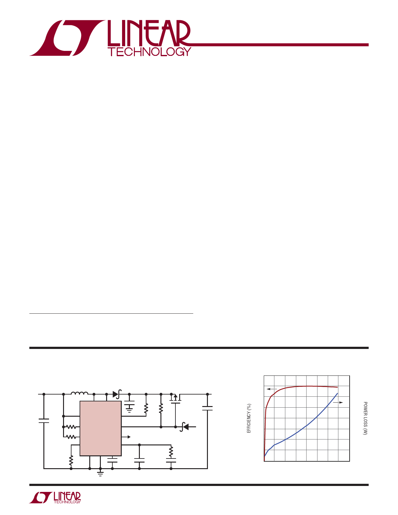
TYPICAL APPLICATION
1MHz, 5V to 12V Boost Converter with Output Short Circuit Protection
2.2μH
VIN
5V
SW1 SW2
10μF
130k 6.3k
VIN
22μF 100k FAULT
FB
GATE
200k
LT3579
SHDN
CLKOUT
RT
VC
TEMPERATURE
MONITOR
SYNC GND SS
8k
VOUT
12V
1.7A
10μF
VIN
86.6k
0.1μF
47pF
2.2nF
3579 TA01
Efficiency and Power Loss
100
3.2
90
2.8
80
2.4
70
2.0
60
1.6
50
1.2
40
0.8
30
0.4
20
0
0 0.25 0.5 0.75 1 1.25 1.5 1.75 2
LOAD CURRENT (A)
35791 TA02
35791f
1
Share Link: 