LT3579IUFD-1-PBF Просмотр технического описания (PDF) - Linear Technology
Номер в каталоге
Компоненты Описание
производитель
LT3579IUFD-1-PBF Datasheet PDF : 40 Pages
| |||
LT3579/LT3579-1
APPLICATIONS INFORMATION
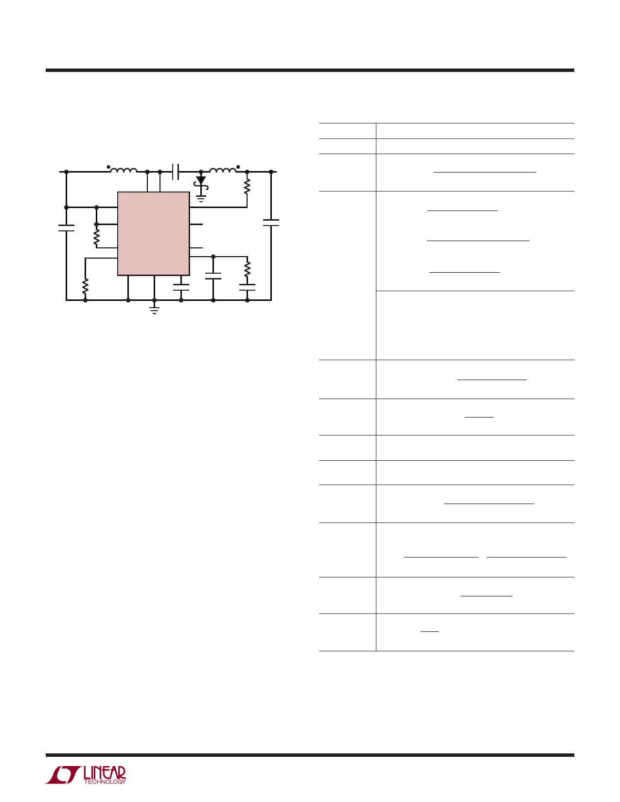
DUAL INDUCTOR INVERTING CONVERTER COMPONENT
SELECTION – COUPLED OR UN-COUPLED INDUCTORS
L1
3.3μH
C1
4.7μF
VIN
5V
CIN
22μF
SW1 SW2
VIN
FB
SHDN
GATE
100k
LT3579
L2
3.3μH
D1
30V, 2A
RFB
144k
VOUT
–12V
1.2A
COUT
10μF
s2
FAULT
CLKOUT
RT
VC
SYNC GND SS
RC
CF
20k
RT
CSS
27pF
CC
72k
0.22μF
1nF
3759 F08
Figure 8. Dual Inductor Inverting Converter – The Component
Values Given Are Typical Values for a 1.2MHz, 5V to –12V Inverting
Topology Using Coupled Inductors
Due to its unique FB pin, the LT3579 can work in a Dual
Inductor Inverting configuration as in Figure 8. Changing
the connections of L2 and the Schottky diode in the
SEPIC topology, results in generating negative output
voltages. This solution results in very low output voltage
ripple due to inductor L2 in series with the output. Output
disconnect is inherently built into this topology due to the
capacitor C1.
Table 3 is a step-by-step set of equations to calculate
component values for the LT3579 when operating as a Dual
Inductor Inverting converter using coupled inductors. Input
parameters are input and output voltage, and switching
frequency (VIN, VOUT and fOSC respectively). Refer to the
Appendix for further information on the design equations
presented in Table 3.
Variable Definitions:
VIN = Input Voltage
VOUT = Output Voltage
DC = Power Switch Duty Cycle
fOSC = Switching Frequency
IOUT = Maximum Output Current
IRIPPLE = Inductor Ripple Current
Table 3. Dual Inductor Inverting Design Equations
PARAMETERS/EQUATIONS
Step 1: Inputs Pick VIN, VOUT, and fOSC to calculate equations below.
Step 2: DC
DC ≅
| VOUT | + 0.5V
VIN + | VOUT |+0.5V – 0.27V
Step 3: L
L TYP
=
(VIN – 0.27V) • DC
fOSC • 1.8A
(1)
LMIN
=
(
VIN – 0.27V) • (2 • DC
4A • fOSC • (1 – DC)
–
1)
(2)
LMAX
=
(VIN – 0.27V) • DC
fOSC • 0.5A
(3)
• Solve equations 1, 2, and 3.
• Choose the higher value between LTYP and LMIN for L.
L should never exceed LMAX.
• L = L1 = L2 for coupled inductors.
• L = L1⏐⏐L2 for un-coupled inductors.
Step 4: IRIPPLE
IRIPPLE
=
(VIN
– 0.27V)
fOSC • L
•
DC
Step 5: IOUT
⎛
IOUT = ⎝⎜6A –
IRIPPLE
2
⎞
⎠⎟
•
(1
–
DC)
Step 6: D1
VR > VIN +| VOUT | ; IAVG > IOUT
Step 7: C1
Step 8: COUT
Step 9: CIN
Step 10: RFB
4.7μF (typical) ; VRATING > VIN + | VOUT |
COUT
=
8
•
fOSC
IRIPPLE
• 0.005 • | VOUT
|
CIN =CPWR +CVIN
CIN
=
8
•
IRIPPLE
fOSC • 0.005
•
VIN
+
40
•
6A • DC
fOSC • 0.005
•
VIN
RFB
=
|
VOUT | + 9mV
83.3μA
Step 11: RT
RT
=
87.6
fOSC
– 1;
fOSC
in
MHz
and RT
in
kΩ
Note: The maximum design target for peak switch current is 6A and
is used in this table. The final values for COUT and CIN may deviate
from the above equations in order to obtain desired load transient
performance for a particular application.
35791f
15
Share Link: 