LT3570(RevA) Просмотр технического описания (PDF) - Linear Technology
Номер в каталоге
Компоненты Описание
производитель
LT3570 Datasheet PDF : 20 Pages
| |||
LT3570
APPLICATIONS INFORMATION
FB Resistor Network
The output voltage is programmed with a resistor divider
(refer to the Block Diagram) between the output and the
FB pin. Choose the resistors according to:
R1=
R2
⎛
⎝⎜
VOUT
788mV
–
1⎞⎠⎟
Buck Inductor Selection and Maximum Output Current
A good first choice for the inductor value is
L
=
VOUT2 + VF
0.75 • f
for SW2
where VF is the voltage drop of the catch diode (~0.4V)
and f is the switching frequency. With this inductance
value or greater, the maximum load current will be 1A,
independent of input voltage. The inductor’s RMS current
rating must be greater than the maximum load current and
its saturation current should be at least 30% higher. For
highest efficiency, the series resistance (DCR) should be
less than 0.1Ω. Table 1 lists several vendors and types
that are suitable.
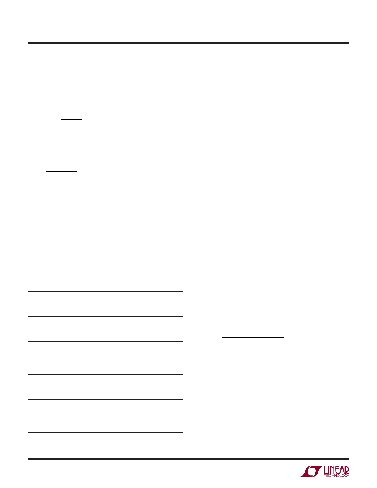
Table 1. Inductors
PART NUMBER
Sumida
CDRH4D28-3R3
CDRH4D28-4R7
CDC5D23-2R2
CR43-3R3
CDRH5D28-100
Coilcraft
DO1608C-332
DO1608C-472
MOS6020-332
D03314-103
D03314-222
Toko
(D62F)847FY-2R4M
(D73LF)817FY-2R2M
Coiltronics
TP3-4R7
TP1-2R2
TP4-100
VALUE
ISAT
(μH)
(A)
3.3
1.57
4.7
1.32
2.2
2.50
3.3
1.44
10
1.3
3.3
2.00
4.7
1.50
3.3
1.8
10
0.8
2.2
1.6
2.4
2.5
2.2
2.7
4.7
1.5
2.2
1.3
10
1.5
DCR HEIGHT
(Ω)
(mm)
0.049
3.0
0.072
3.0
0.03
2.5
0.086
3.5
0.048
3.0
0.080
2.9
0.090
2.9
0.046
2.0
0.520
1.4
0.200
1.4
0.037
2.7
0.03
3.0
0.181
2.2
0.188
1.8
0.146
3.0
10
The optimum inductor for a given application may differ
from the one indicated by this simple design guide. A
larger value inductor provides a slightly higher maximum
load current and will reduce the output voltage ripple. If
your load is lower than the maximum load current, then
you can relax the value of the inductor and operate with
higher ripple current. This allows you to use a physically
smaller inductor or one with a lower DCR resulting in
higher efficiency. Be aware that if the inductance differs
from the simple rule above, then the maximum load current
will depend on input voltage. In addition, low inductance
may result in discontinuous mode operation, which further
reduces maximum load current. For details of maximum
output current and discontinuous mode operation, see
Linear Technology’s Application Note 44. Finally, for duty
cycles greater than 50% (VOUT2/VIN2 > 0.5) a minimum
inductance is required to avoid subharmonic oscillations,
see Application Note 19.
The current in the inductor is a triangle wave with an average
value equal to the load current. The peak switch current
is equal to the output current plus half the peak-to-peak
inductor ripple current. The LT3570 limits its switch cur-
rent in order to protect itself and the system from overload
faults. Therefore, the maximum output current that the
LT3570 will deliver depends on the switch current limit,
the inductor value and the input and output voltages.
When the switch is off, the potential across the inductor
is the output voltage plus the catch diode drop. This gives
the peak-to-peak ripple current in the inductor:
( ) ΔIL2
=
(1–
DC2) VOUT
L•f
2
+
VF
where DC2 is the duty cycle and is defined as:
DC2 =
VOUT2
VIN2
The peak inductor and switch current is:
ISWPK 2
= ILPK2
=
IOUT2
+
ΔIL2
2
To maintain output regulation, this peak current must be
less than the LT3570’s switch current limit ILIM2. ILIM2 is
at least 1.5A at low duty cycles and decreases linearly
3570fa
Share Link: 