LT3483IDC-TRPBF Просмотр технического описания (PDF) - Linear Technology
Номер в каталоге
Компоненты Описание
производитель
LT3483IDC-TRPBF Datasheet PDF : 12 Pages
| |||
LT3483/LT3483A
APPLICATIONS INFORMATION
Board Layout Considerations
As with all switching regulators, careful attention must
be given to the PCB board layout and component place-
ment. Proper layout of the high frequency switching path
is essential. The voltage signals of the SW and D pins
have sharp rising and falling edges. Minimize the length
and area of all traces connected to the SW and D pins.
In particular, it is desirable to minimize the trace length
to and from the flying capacitor, since current in this ca-
pacitor switches directions within a cycle. Always use a
ground plane under the switching regulator to minimize
interplane coupling.
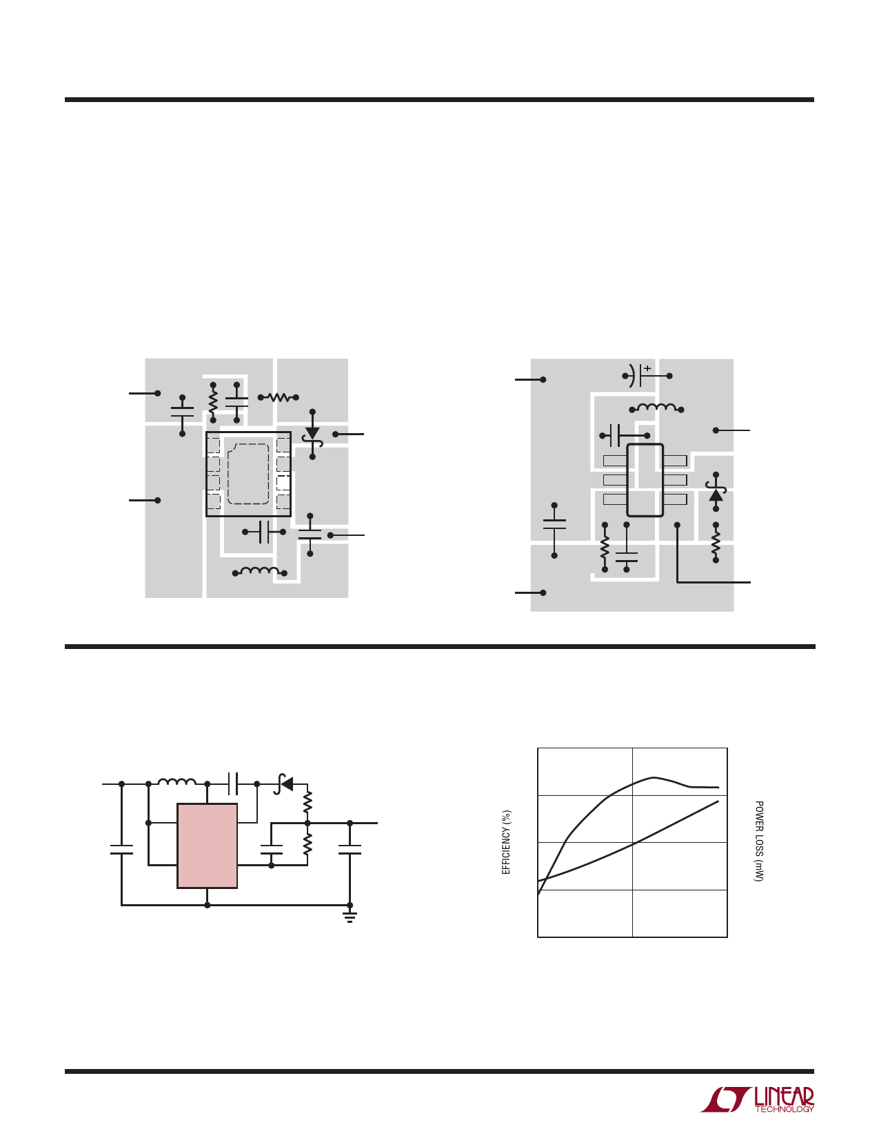
Suggested Layout (DFN)
for Inverting Charge Pump
VOUT
GND
COUT
R1
1
2
3
4
8
7
9
6
5
CIN
L1
A
SHDN
K
VIN
CFLY
3483 AI02
Suggested Layout (SOT-23)
for Inverting Charge Pump
GND
CIN L1
CFLY
VIN
1
6
2
5
3
4
COUT
R1
VOUT
SHDN
3483 AI01
TYPICAL APPLICATIONS
VIN
3.6V
C1
4.7µF
3.6V to –22V DC/DC Converter
C2
L1
10µH
0.1µF
D1
SW
VIN
D
LT3483
SHDN FB
GND
RS
30Ω
R1
5pF 2.2M
VOUT
–22V
8mA
C3
1µF
C1: TAIYO YUDEN LMK316BJ475MD
C2: TAIYO YUDEN TMK107BJ104 (X5R)
C3: TAIYO YUDEN TMK316BJ105MD
D1: PHILIPS PMEG3002AEB
L1: MURATA LQH2MCN100K02L
3483 TA02a
3.6V to –22V Converter Efficiency and Power Loss
75
1000
EFFICIENCY
70
100
65
10
POWER
LOSS
60
1
55
0.1
1
LOAD CURRENT (mA)
0.1
10
3483 TA02b
3483fc
8
Share Link: 