LT3483IDC-TRPBF Просмотр технического описания (PDF) - Linear Technology
Номер в каталоге
Компоненты Описание
производитель
LT3483IDC-TRPBF Datasheet PDF : 12 Pages
| |||
LT3483/LT3483A
PIN FUNCTIONS (DFN/TSOT-23)
FB (Pin 1/Pin 3): Feedback. Place resistor to negative
output here. Set resistor value R1 = VOUT/10µA.
GND (Pins 2, 3/Pin 2): Ground. For DFN package, tie both
pin 2 and pin 3 together to ground.
SW (Pin 4/Pin 1): Switch. Connect to external inductor
L1 and positive terminal of transfer capacitor.
VIN (Pin 5/Pin 6): Input Supply. Must be locally bypassed
with 1µF or greater.
NC (Pin 6/NA): No Internal Connection.
D (Pin 7/Pin 5): Anode Terminal of Integrated Schottky
Diode. Connect to negative terminal of transfer capaci-
tor and external inductor L2 (flyback configuration) or
to cathode of external Schottky diode (inverting charge
pump configuration).
SHDN (Pin 8/Pin 4): Shutdown. Connect to GND to turn
device off. Connect to supply to turn device on.
Exposed Pad (Pin 9/NA): GND. The exposed pad should
be soldered to the PCB ground to achieve the rated thermal
performance.
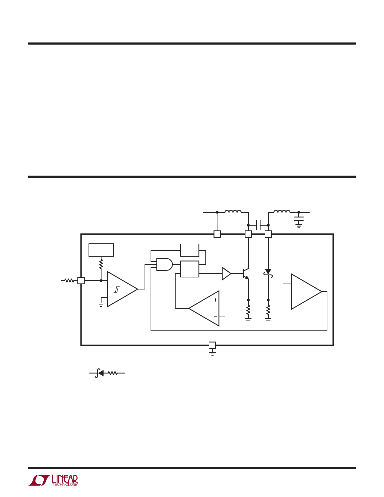
BLOCK DIAGRAM
1.250V
REFERENCE
125k
R1
FB
VOUT
3
+
A3
–
OPTIONAL CHARGE PUMP CONFIGURATION.
L1B REPLACED WITH:
D2 R2
D
VOUT
L1A
L1B
VIN
•
CFLY
•
VOUT
COUT
6
VIN
300ns
DELAY
SQ
RQ
1
5
SW
D
Q1
D1
25mV
A1
0.1Ω
0.1Ω
20mV
(LT3483)
+
A2
–
GND
2
PIN NUMBERS CORRESPOND TO THE
6-PIN TSOT-23 PACKAGE
3483 BD
3483fc
5
Share Link: 