LT3462 Просмотр технического описания (PDF) - Linear Technology
Номер в каталоге
Компоненты Описание
производитель
LT3462 Datasheet PDF : 8 Pages
| |||
LT3462/LT3462A
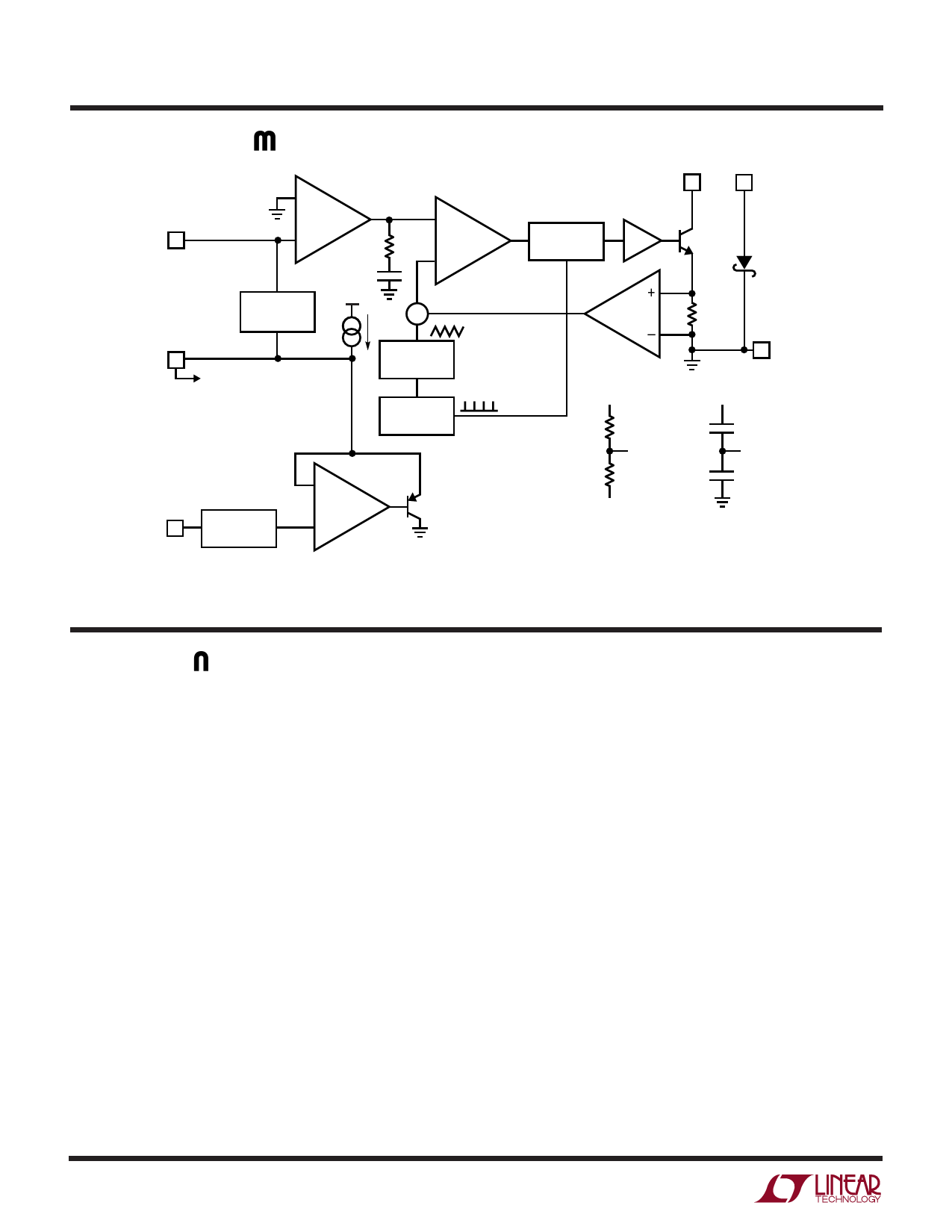
BLOCK DIAGRA
FB 3
–
A1
E AMP
+
SDREF 4
SHUTDOWN
BIAS CURRENT
CANCELLATION
OFF → 3µA
ON → 180µA
SHUTDOWN
–
A2
RC
COMP
+
CC
∑
ISRC
RAMP
GENERATOR
1.2MHz*
OSCILLATOR
*LT3462A IS 2.7MHz
–
Q2
VIN 6
1.265V
REFERENCE
+
DRIVER
R
Q
S
1 SW 5 D
Q1
0.1Ω
DO
LG
2 GND
VOUT
VOUT
R1 (EXTERNAL)
FB
R2 (EXTERNAL)
CS1 (EXTERNAL)
SDREF
CS2 (EXTERNAL)
SDREF
CS1, CS2 OPTIONAL SOFT-START COMPONENTS
3462 F02
Figure 1. Block Diagram
U
OPERATIO
The LT3462 uses a constant frequency, current mode
control scheme to provide excellent line and load regula-
tion. Operation can be best understood by referring to the
Block Diagram in Figure 1. At the start of each oscillator
cycle, the SR latch is set, turning on the power switch Q1.
A voltage proportional to the switch current is added to a
stabilizing ramp and the resulting sum is fed into the
positive terminal of the PWM comparator. When this
voltage exceeds the voltage at the output of the EAMP, the
SR latch is reset, turning off the power switch. The level
at the output of the EAMP is simply an amplified version
of the difference between the feedback voltage and GND.
In this manner, the error amplifier sets the correct peak
current level to keep the output in regulation. If the error
amplifier’s output increases, more current is taken from
the output; if it decreases, less current is taken. One
function not shown in Figure 1 is the current limit. The
switch current is constantly monitored and not allowed to
exceed the nominal value of 400mA. If the switch current
reaches 400mA, the SR latch is reset regardless of the
output state of the PWM comparator. This current limit cell
protects the power switch as well as various external
components connected to the LT3462.
SDREF is a dual function input pin. When driven low it
shuts the part down, reducing quiescent supply current to
less than 10µA. When not driven low, the SDREF pin has an
internal pull-up current that turns the regulator on. Once
the part is enabled, the SDREF pin sources up to
180µA nominally at a fixed voltage of 1.265V through
external resistor R2 to FB. If there is no fault condition
present, FB will regulate to 0V, and VOUT will regulate to
1.265V • (–R1/R2). An optional soft-start circuit uses the
fixed SDREF pull-up current and a capacitor from SDREF
to VOUT to set the dV/dt on VOUT. In shutdown, an FB bias
current cancellation circuit supplies up to 150µA biasing
current to external resistor R1 while VOUT is lower than FB.
This function eliminates R2 loading of SDREF during
shutdown. As a result, supply current in shutdown may
exceed 10µA by the amount of current flowing in R1.
3462af
4
Share Link: 