LT1817 –Я—А–Њ—Б–Љ–Њ—В—А —В–µ—Е–љ–Є—З–µ—Б–Ї–Њ–≥–Њ –Њ–њ–Є—Б–∞–љ–Є—П (PDF) - Linear Technology
–Э–Њ–Љ–µ—А –≤ –Ї–∞—В–∞–ї–Њ–≥–µ
–Ъ–Њ–Љ–њ–Њ–љ–µ–љ—В—Л –Ю–њ–Є—Б–∞–љ–Є–µ
–њ—А–Њ–Є–Ј–≤–Њ–і–Є—В–µ–ї—М
LT1817
Linear Technology

LT1817 Datasheet PDF : 20 Pages
| |||
LT1815
LT1816/LT1817
ELECTRICAL CHARACTERISTICS The q denotes the specifications which apply over the full operating
temperature range, otherwise specifications are at TA = 25°C (Note 8). VS = 5V, 0V; VCM = 2.5V, RL to 2.5V unless otherwise noted.
For the programmable current option (LT1815S6 or LT1816A), the ISET pin must be connected to V вАУ through 75вД¶ or less, unless
otherwise noted.
SYMBOL PARAMETER
ISET
ISET Pin Current (Note 10)
CONDITIONS
LT1815S6/LT1816A
TA = 0°C to 70°C
TA = вАУ 40¬∞C to 85¬∞C
MIN TYP MAX UNITS
вАУ150 вАУ 100
µA
q вАУ175
µA
q вАУ200
µA
Note 1: Absolute Maximum Ratings are those values beyond which the life
of a device may be impaired.
Note 2: Differential inputs of ±6V are appropriate for transient operation
only, such as during slewing. Large sustained differential inputs can cause
excessive power dissipation and may damage the part.
Note 3: A heat sink may be required to keep the junction temperature
below absolute maximum when the output is shorted indefinitely.
Note 4: Input offset voltage is pulse tested and is exclusive of warm-up
drift.
Note 5: Slew rate is measured between ±2V at the output with ±3V input
for ±5V supplies and 2VP-P at the output with a 3VP-P input for single 5V
supplies.
Note 6: Full-power bandwidth is calculated from the slew rate:
FPBW = SR/2ѕАVP.
Note 7: This parameter is not 100% tested.
Note 8: The LT1815C/LT1816C/LT1817C are guaranteed to meet specified
performance from 0°C to 70°C and are designed, characterized and
expected to meet the extended temperature limits, but are not tested at
вАУ 40¬∞C and 85¬∞C. The LT1815I/LT1816I/LT1817I are guaranteed to meet
the extended temperature limits.
Note 9: Thermal resistance (ќЄJA) varies with the amount of PC board metal
connected to the package. The specified values are for short traces
connected to the leads. If desired, the thermal resistance can be
substantially reduced by connecting Pin 2 of the SOT-23, Pin 4 of the
SO-8 and MS8, Pin 5 of the MS10 or the underside metal of the DD
package to a large metal area.
Note 10: A resistor of 40k or less is required between the ISET and VвАУ pins
of the LT1815S6 and the LT1816AMS. See the applications section for
information on selecting a suitable resistor.
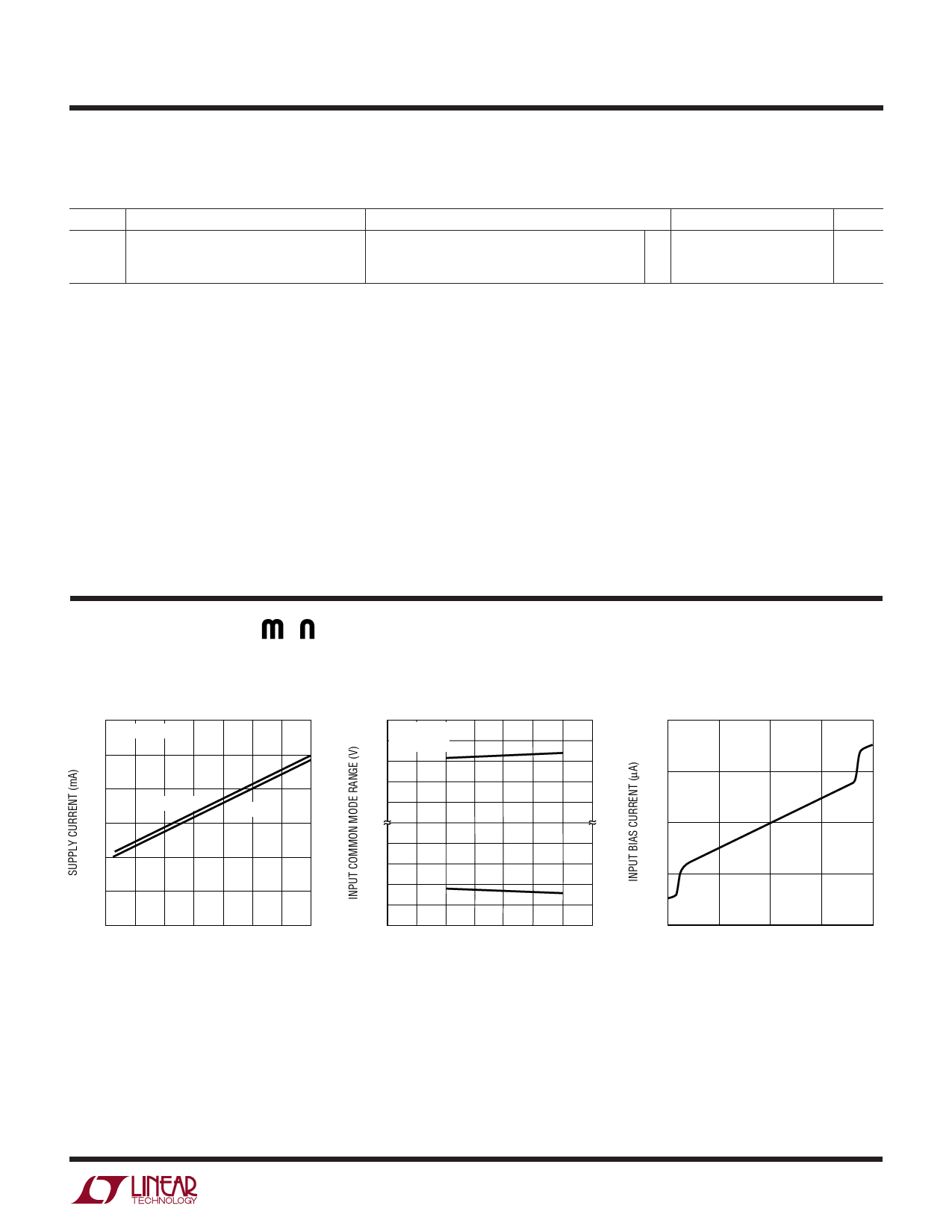
TYPICAL PERFOR A CE CHARACTERISTICS
Supply Current vs Temperature
12
PER AMPLIFIER
10
8
VS = ±5V
VS = ±2.5V
6
4
2
0
вАУ50 вАУ25
0 25 50 75
TEMPERATURE (°C)
100 125
181567 G01
Input Common Mode Range
vs Supply Voltage
V+
TA = 25°C
вАУ 0.5 вИЖVOS < 1mV
вАУ1.0
вАУ1.5
вАУ 2.0
2.0
1.5
1.0
0.5
VвАУ
0
1 2 34 5 6 7
SUPPLY VOLTAGE (± V)
181567 G02
Input Bias Current
vs Common Mode Voltage
0
TA = 25°C
VS = ± 5V
вАУ1
вАУ2
вАУ3
вАУ4
вАУ 5.0
вАУ 2.5
0
2.5
5.0
INPUT COMMON MODE VOLTAGE (V)
181567 G03
181567fa
7
Share Link: