LT1812 –ü—Ä–ĺ—Ā–ľ–ĺ—ā—Ä —ā–Ķ—Ö–Ĺ–ł—á–Ķ—Ā–ļ–ĺ–≥–ĺ –ĺ–Ņ–ł—Ā–į–Ĺ–ł—Ź (PDF) - Linear Technology
–Ě–ĺ–ľ–Ķ—Ä –≤ –ļ–į—ā–į–Ľ–ĺ–≥–Ķ
–ö–ĺ–ľ–Ņ–ĺ–Ĺ–Ķ–Ĺ—ā—č –ě–Ņ–ł—Ā–į–Ĺ–ł–Ķ
–Ņ—Ä–ĺ–ł–∑–≤–ĺ–ī–ł—ā–Ķ–Ľ—Ć
LT1812 Datasheet PDF : 16 Pages
| |||
LT1812
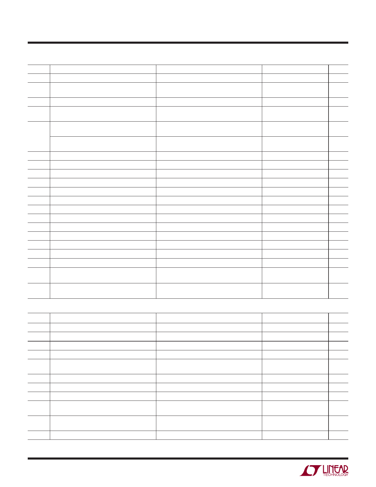
ELECTRICAL CHARACTERISTICS TA = 25¬įC, VS = ¬Ī5V, VCM = 0V unless otherwise noted (Note 10).
SYMBOL PARAMETER
CIN
Input Capacitance
VCM
Input Voltage Range (Positive)
Input Voltage Range (Negative)
CMRR Common Mode Rejection Ratio
AVOL
Large-Signal Voltage Gain
VOUT
Maximum Output Swing (Positive)
Maximum Output Swing (Negative)
IOUT
ISC
SR
FPBW
GBW
tr, tf
OS
tPD
ts
THD
ROUT
ISHDN
Maximum Output Current
Output Short-Circuit Current
Slew Rate
Full Power Bandwidth
Gain Bandwidth Product
Rise Time, Fall Time
Overshoot
Propagation Delay
Settling Time
Total Harmonic Distortion
Differential Gain
Differential Phase
Output Resistance
SHDN Pin Current
IS
Supply Current
CONDITIONS
MIN TYP MAX
2
3.5
4
1
1.5
VCM = 1.5V to 3.5V
73
82
VOUT = 1.5V to 3.5V, RL = 500ő©
VOUT = 1.5V to 3.5V, RL = 100ő©
1.0
2.0
0.7
1.5
RL = 500ő©, 30mV Overdrive
RL = 100ő©, 30mV Overdrive
RL = 500ő©, 30mV Overdrive
RL = 100ő©, 30mV Overdrive
VOUT = 3.5V or 1.5V, 30mV Overdrive
3.9
4.1
3.7
3.9
0.9
1.1
1.1
1.3
¬Ī 25 ¬Ī40
VOUT = 2.5V, 1V Overdrive (Note 3)
AV = ‚Äď1 (Note 5)
1V Peak (Note 6)
¬Ī55
¬Ī80
200
350
55
f = 200kHz
65
94
AV = 1, 10% to 90%, 0.1V, RL = 100ő©
2.1
AV = 1, 0.1V, RL = 100ő©
25
AV = 1, 50% VIN to 50% VOUT, 0.1V, RL = 100ő©
3
2V Step, 0.1%, AV = ‚Äď1
30
f = 1MHz, VOUT = 2VP-P, AV = 2, RL = 500ő©
‚Äď 75
VOUT = 2VP-P, AV = 2, RL = 150ő©
0.22
VOUT = 2VP-P, AV = 2, RL = 150ő©
0.21
AV = 1, f = 1MHz
0.45
SHDN > V ‚Äď + 2.0V (On) (Note 11)
SHDN < V‚Äď + 0.4V (Off) (Note 11)
0
¬Ī1
‚Äď50
‚Äď20
SHDN > V‚Äď + 2.0V (On) (Note 11)
SHDN < V‚Äď + 0.4V (Off) (Note 11)
2.7
3.6
20
50
0¬įC ‚ȧ TA ‚ȧ 70¬įC, VS = ¬Ī 5V, VCM = 0V unless otherwise noted (Note 10).
SYMBOL PARAMETER
CONDITIONS
VOS
őĒVOS/őĒT
IOS
IB
VCM
Input Offset Voltage
Input Offset Voltage Drift
Input Offset Current
Input Bias Current
Input Voltage Range (Positive)
Input Voltage Range (Negative)
(Note 4)
(Note 7)
CMRR
Common Mode Rejection Ratio
Minimum Supply Voltage
VCM = ¬Ī3.5V
PSRR
AVOL
VOUT
IOUT
Power Supply Rejection Ratio
Large-Signal Voltage Gain
Maximum Output Swing
Maximum Output Current
VS = ¬Ī2V to ¬Ī5.5V
VOUT = ¬Ī3V, RL = 500ő©
VOUT = ¬Ī3V, RL = 100ő©
RL = 500ő©, 30mV Overdrive
RL = 100ő©, 30mV Overdrive
VOUT = ¬Ī3V, 30mV Overdrive
MIN TYP MAX
2
10
15
500
¬Ī5
3.5
‚Äď3.5
73
¬Ī2
76
1.0
0.7
¬Ī3.70
¬Ī3.25
¬Ī35
UNITS
pF
V
V
dB
V/mV
V/mV
V
V
V
V
mA
mA
V/őľs
MHz
MHz
ns
%
ns
ns
dB
%
DEG
ő©
őľA
őľA
mA
őľA
UNITS
mV
őľV/¬įC
nA
őľA
V
V
dB
V
dB
V/mV
V/mV
V
V
mA
1812fb
4
Share Link: 