LT1678IS8 Просмотр технического описания (PDF) - Linear Technology
Номер в каталоге
Компоненты Описание
производитель
LT1678IS8 Datasheet PDF : 16 Pages
| |||
LT1678/LT1679
APPLICATIO S I FOR ATIO
Rail-to-Rail Operation
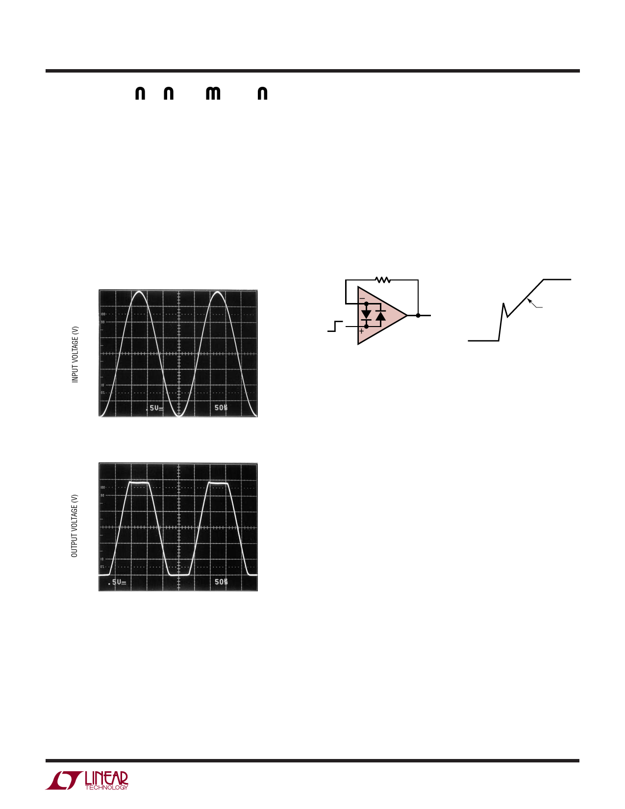
To take full advantage of an input range that can exceed
the supply, the LT1678/LT1679 are designed to eliminate
phase reversal. Referring to the photographs shown in
Figure 1, the LT1678/LT1679 are operating in the fol-
lower mode (AV = +1) at a single 3V supply. The output
of the LT1678/LT1679 clips cleanly and recovers with no
phase reversal. This has the benefit of preventing lock-up
in servo systems and minimizing distortion components.
Input = –0.5V to 3.5V
3
2
1
0
– 0.5
50µs/DIV
16789 F01a
LT1678 Output
3
2
1
0
– 0.5
50µs/DIV
16789 F01b
Figure 1. Voltage Follower with Input Exceeding the Supply
Voltage (VS = 3V)
Unity-Gain Buffer Application
When RF ≤ 100Ω and the input is driven with a fast, large-
signal pulse (>1V), the output waveform will look as
shown in the pulsed operation diagram (Figure 2).
During the fast feedthrough-like portion of the output, the
input protection diodes effectively short the output to the
input and a current, limited only by the output short-circuit
protection, will be drawn by the signal generator. With
RF ≥ 500Ω, the output is capable of handling the current
requirements (IL ≤ 20mA at 10V) and the amplifier stays
in its active mode and a smooth transition will occur.
As with all operational amplifiers when RF > 2k, a pole will
be created with RF and the amplifier’s input capacitance,
creating additional phase shift and reducing the phase
margin. A small capacitor (20pF to 50pF) in parallel with RF
will eliminate this problem.
RF
–
OUTPUT
+
LT1678
6V/µs
16789 F02
Figure 2. Pulsed Operation
Noise Testing
The 0.1Hz to 10Hz peak-to-peak noise of the LT1678/
LT1679 are measured in the test circuit shown (Figure 3).
The frequency response of this noise tester (Figure 4)
indicates that the 0.1Hz corner is defined by only one zero.
The test time to measure 0.1Hz to 10Hz noise should not
exceed ten seconds, as this time limit acts as an additional
zero to eliminate noise contributions from the frequency
band below 0.1Hz.
Measuring the typical 90nV peak-to-peak noise perfor-
mance of the LT1678/LT1679 requires special test pre-
cautions:
1. The device should be warmed up for at least five
minutes. As the op amp warms up, its offset voltage
changes typically 3µV due to its chip temperature
increasing 10°C to 20°C from the moment the power
supplies are turned on. In the ten-second measurement
interval these temperature-induced effects can easily
exceed tens of nanovolts.
2. For similar reasons, the device must be well shielded
from air currents to eliminate the possibility of
thermoelectric effects in excess of a few nanovolts,
which would invalidate the measurements.
sn16789 16789fs
11
Share Link: 