LT1121ACS8(RevA) Просмотр технического описания (PDF) - Linear Technology
Номер в каталоге
Компоненты Описание
производитель
LT1121ACS8 Datasheet PDF : 12 Pages
| |||
LT1121/LT1121-3.3/LT1121-5
TYPICAL PERFOR A CE CHARACTERISTICS
Load Regulation
0
∆ILOAD = 1mA TO 150mA
–5
–10
LT1121*
LT1121-3.3
–15
– 20
– 25
LT1121-5
– 30
–35 * ADJ PIN TIED TO
OUTPUT PIN
– 40
–50 –25 0 25 50 75
TEMPERATURE (°C)
100 125
1121 G21
LT1121-5
Load Transient Response
0.2 VIN = 6V
CIN = 0.1µF
0.1 COUT = 1µF
0
– 0.1
– 0.2
150
100
0 0.1 0.2 0.3 0.4 0.5 0.6 0.7 0.8 0.9 1.0
TIME (ms)
1121 G30
LT1121-5
Load Transient Response
0.2
VIN = 6V
CIN = 0.1µF
0.1 COUT = 3.3µF
0
– 0.1
– 0.2
150
100
50
0 0.1 0.2 0.3 0.4 0.5 0.6 0.7 0.8 0.9 1.0
TIME (ms)
1121 G31
PI FU CTIO S
Input Pin: Power is supplied to the device through the
input pin. The input pin should be bypassed to ground if
the device is more than 6 inches away from the main input
filter capacitor. In general the output impedance of a
battery rises with frequency so it is usually adviseable to
include a bypass capacitor in battery-powered circuits. A
bypass capacitor in the range of 0.1µF to 1µF is sufficient.
The LT1121 is designed to withstand reverse voltages on
the input pin with respect to both ground and the output
pin. In the case of a reversed input, which can happen if a
battery is plugged in backwards, the LT1121 will act as if
there is a diode in series with its input. There will be no
reverse current flow into the LT1121 and no reverse
voltage will appear at the load. The device will protect both
itself and the load.
Output Pin: The output pin supplies power to the load. An
output capacitor is required to prevent oscillations. See
the Applications Information section for recommended
value of output capacitance and information on reverse
output characteristics.
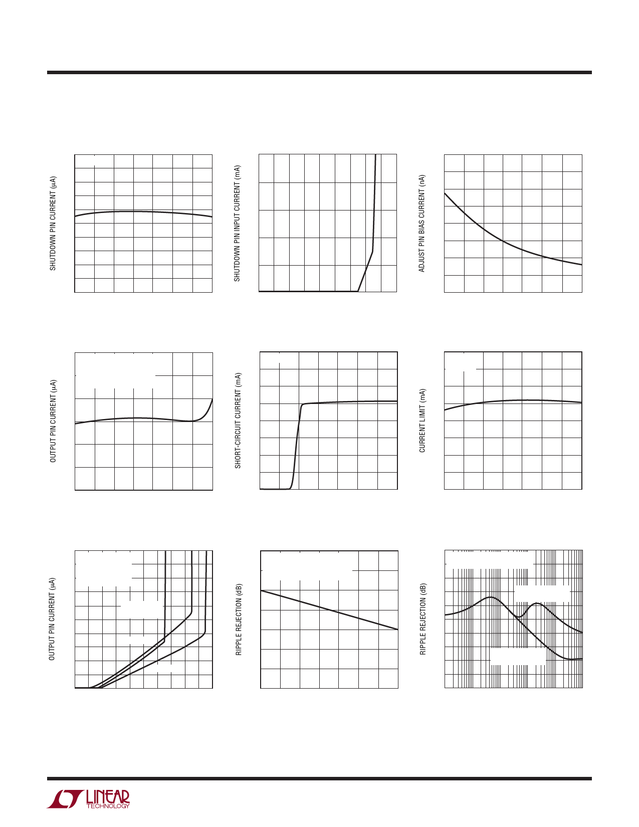
Shutdown Pin: This pin is used to put the device into
shutdown. In shutdown the output of the device is turned
off. This pin is active low. The device will be shut down if
the shutdown pin is pulled low. The shutdown pin current
with the pin pulled to ground will be 6µA. The shutdown
pin is internally clamped to 7V and – 0.6V (one VBE). This
allows the shutdown pin to be driven directly by 5V logic
or by open collector logic with a pull-up resistor. The pull-
up resistor is only required to supply the leakage current
of the open collector gate, normally several microam-
peres. Pull-up current must be limited to a maximum of
20mA. A curve of shutdown pin input current as a function
of voltage appears in the Typical Performance Character-
istics. If the shutdown pin is not used it can be left open
circuit. The device will be active, output on, if the shutdown
pin is not connected.
Adjust Pin: For the adjustable LT1121, the adjust pin is the
input to the error amplifier. This pin is internally clamped
to 6V and – 0.6V (one VBE). It has a bias current of 150nA
which flows into the pin. See Bias Current curve in the
Typical Performance Characteristics. The adjust pin refer-
ence voltage is 3.75V referenced to ground. The output
voltage range that can be produced by this device is 3.75V
to 30V.
7
Share Link: 