LT1576CS8-SYNC Просмотр технического описания (PDF) - Linear Technology
Номер в каталоге
Компоненты Описание
производитель
LT1576CS8-SYNC Datasheet PDF : 28 Pages
| |||
LT1576/LT1576-5
ABSOLUTE MAXIMUM RATINGS
(Note 1)
Input Voltage .......................................................... 25V
BOOST Pin Above Input Voltage ............................. 10V
SHDN Pin Voltage ..................................................... 7V
BIAS Pin Voltage ...................................................... 7V
FB Pin Voltage (Adjustable Part) ............................ 3.5V
FB Pin Current (Adjustable Part) ............................ 1mA
SYNC Pin Voltage ..................................................... 7V
Operating Junction Temperature Range
LT1576C ............................................... 0°C to 125° C
LT1576I ........................................... – 40°C to 125°C
Storage Temperature Range ................ – 65°C to 150°C
Lead Temperature (Soldering, 10 sec)................. 300°C
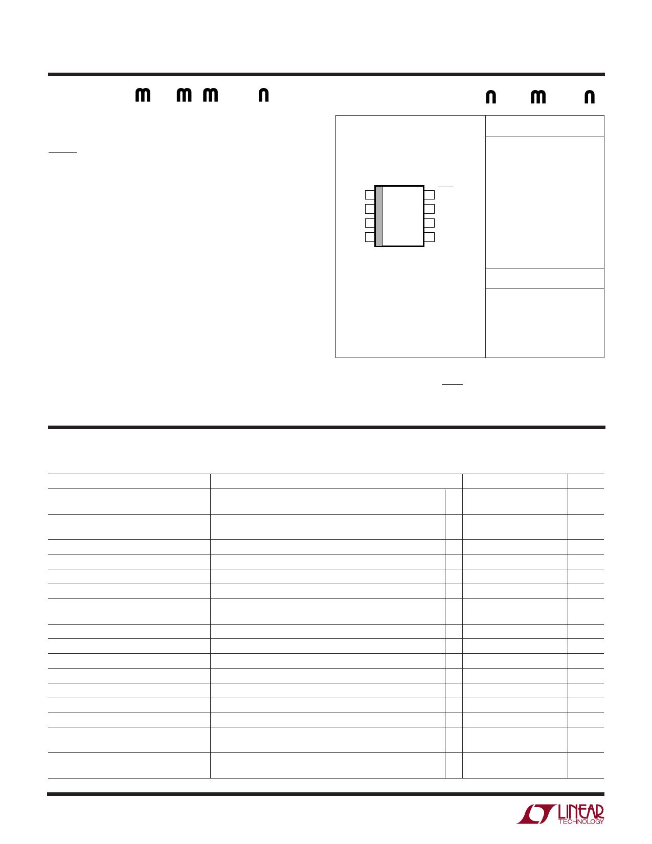
PACKAGE/ORDER INFORMATION
ORDER PART NUMBER
VSW 1
VIN 2
BOOST 3
GND 4
TOP VIEW
8
SHDN OR
SYNC*
7 FB OR SENSE*
6 VC
5 BIAS
S8 PACKAGE
8-LEAD PLASTIC SO
θJA = 80°C/ W WITH FUSED GROUND PIN
CONNECTED TO GROUND PLANE OR
LARGE LANDS
LT1576CS8
LT1576CS8-SYNC
LT1576IS8
LT1576IS8-SYNC
LT1576CS8-5
LT1576CS8-5 SYNC
LT1576IS8-5
LT1576IS8-5 SYNC
S8 PART MARKING
1576
1576SN
1576I
576ISN
15765
5765SN
1576I5
76I5SN
*Default is the adjustable output voltage device with FB pin and shutdown
function. Option -5 replaces FB with SENSE pin for fixed 5V output
applications. -SYNC replaces SHDN with SYNC pin for applications
requiring synchronization. Consult factory for Military grade parts.
ELECTRICAL CHARACTERISTICS The q denotes specifications which apply over the full operating temperature
range, otherwise specifications are TA, TJ = 25°C, VIN = 15V, VC = 1.5V, Boost = VIN + 5V, switch open, unless otherwise noted.
PARAMETER
CONDITIONS
MIN TYP MAX
UNITS
Feedback Voltage
All Conditions
1.195 1.21 1.225
V
q 1.18
1.24
V
Sense Voltage (Fixed 5V)
All Conditions
4.94 5.0 5.06
V
q 4.90
5.10
V
SENSE Pin Resistance
13 18.5 26
kΩ
Reference Voltage Line Regulation
Feedback Input Bias Current
5V ≤ VIN ≤ 25V
0.01 0.03
%/V
q
0.5 2
µA
Error Amplifier Voltage Gain
(Notes 2, 8)
200 400
Error Amplifier Transconductance
∆I (VC) = ±10µA (Note 8)
800 1050 1300
q 400
1700
µMho
µMho
VC Pin to Switch Current Transconductance
Error Amplifier Source Current
Error Amplifier Sink Current
VC Pin Switching Threshold
VC Pin High Clamp
Switch Current Limit
Slope Compensation (Note 9)
VFB = 1.1V
VFB = 1.4V
Duty Cycle = 0
VC Open, VFB = 1.1V, DC ≤ 50%
DC = 80%
1.5
A/ V
q 40 110 190
µA
q 50 130 200
µA
0.8
V
2.1
V
q 1.5 2 3.50
A
0.3
A
Switch On Resistance (Note 7)
ISW = 1.5A
0.2 0.35
Ω
q
0.45
Ω
Maximum Switch Duty Cycle
VFB = 1.1V
90 94
%
q 86 94
%
2
Share Link: 