LT1469AIDF-2-TRPBF –Я—А–Њ—Б–Љ–Њ—В—А —В–µ—Е–љ–Є—З–µ—Б–Ї–Њ–≥–Њ –Њ–њ–Є—Б–∞–љ–Є—П (PDF) - Linear Technology
–Э–Њ–Љ–µ—А –≤ –Ї–∞—В–∞–ї–Њ–≥–µ
–Ъ–Њ–Љ–њ–Њ–љ–µ–љ—В—Л –Ю–њ–Є—Б–∞–љ–Є–µ
–њ—А–Њ–Є–Ј–≤–Њ–і–Є—В–µ–ї—М
LT1469AIDF-2-TRPBF Datasheet PDF : 12 Pages
| |||
LT1469-2
APPLICATIONS INFORMATION
Input Considerations
Each input of the LT1469 is protected with a 100ќ© series
resistor and back-to-back diodes across the bases of
the input devices. If large differential input voltages are
anticipated, limit the input current to less than 10mA with
an external series resistor. Each input also has two ESD
clamp diodesвАФone to each supply. If an input is driven
beyond the supply, limit the current with an external resis-
tor to less than 10mA.
The LT1469 employs bias current cancellation at the inputs.
The inverting input current is trimmed at zero common
mode voltage to minimize errors in inverting applications
such as I-to-V converters. The noninverting input current
is not trimmed and has a wider variation and therefore a
larger maximum value. As the input offset current can be
greater than either input current, the use of balanced source
resistance is NOT recommended as it actually degrades
DC accuracy and also increases noise.
The input bias currents vary with common mode voltage.
The cancellation circuitry was not designed to track this
common mode voltage because the settling time would
have been adversely affected.
The LT1469 inputs can be driven to the negative supply
and to within 0.5V of the positive supply without phase
reversal. As the input moves closer than 0.5V to the posi-
tive supply, the output reverses phase.
Total Input Noise
The total input noise of the LT1469 is optimized for a source
resistance between 1k and 20k. Within this range, the
total input noise is dominated by the noise of the source
resistance itself. When the source resistance is below
1k, voltage noise of the ampliпђБer dominates. When the
source resistance is above 20k, the input noise current is
the dominant contributor.
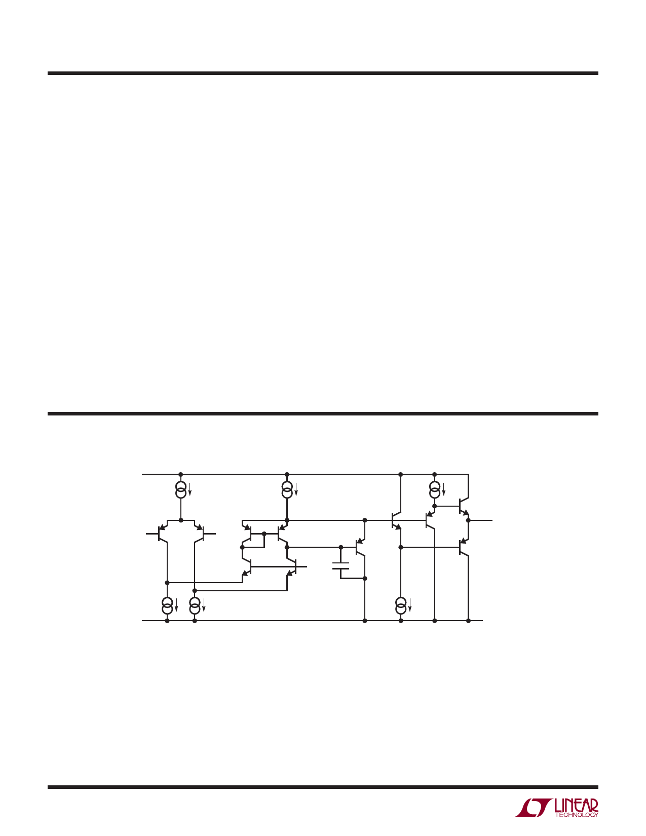
SIMPLIFIED SCHEMATIC
V+
I1
+IN
Q1 Q2
вАУIN Q5
Q3
I2
Q6
Q4
BIAS
Q7
C
I5
Q8
Q9
Q10
OUT
Q11
I3
I4
VвАУ
I6
14692 SS
14692f
10
Share Link: 