LT1469IDF-PBF(RevA) –Я—А–Њ—Б–Љ–Њ—В—А —В–µ—Е–љ–Є—З–µ—Б–Ї–Њ–≥–Њ –Њ–њ–Є—Б–∞–љ–Є—П (PDF) - Linear Technology
–Э–Њ–Љ–µ—А –≤ –Ї–∞—В–∞–ї–Њ–≥–µ
–Ъ–Њ–Љ–њ–Њ–љ–µ–љ—В—Л –Ю–њ–Є—Б–∞–љ–Є–µ
–њ—А–Њ–Є–Ј–≤–Њ–і–Є—В–µ–ї—М
LT1469IDF-PBF Datasheet PDF : 20 Pages
| |||
LT1469
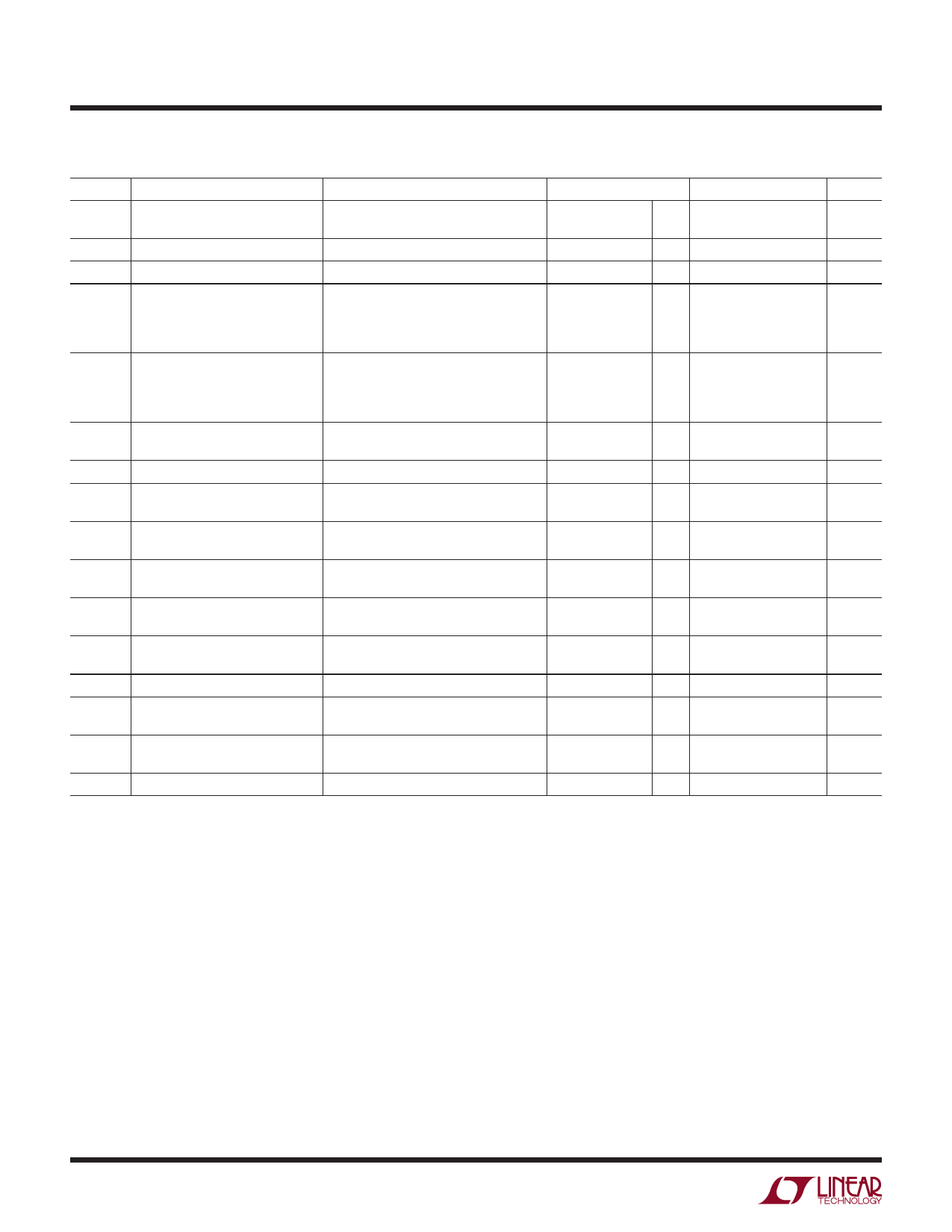
ELECTRICAL CHARACTERISTICS The l denotes the speciпђБcations which apply over the full operating
temperature range, вАУ40¬∞C вЙ§ TA вЙ§ 85¬∞C, VCM = 0V unless otherwise noted. (Note 5)
SYMBOL PARAMETER
CMRR Common Mode Rejection Ratio
PSRR
AVOL
Minimum Supply Voltage
Power Supply Rejection Ratio
Large-Signal Voltage Gain
VOUT
Maximum Output Swing
IOUT
Maximum Output Current
ISC
Output Short-Circuit Current
SR
Slew Rate
CONDITIONS
VCM = ±12.5V
VCM = ±2.5V
Guaranteed by PSRR
VS = ±4.5V to ±15V
VOUT = ±12,5V, RL = 10k
VOUT = ±12.5V, RL = 2k
VOUT = ±2.5V, RL = 10k
VOUT = ±2.5V, RL = 2k
RL = 10k, 1mV Overdrive
RL = 2k, 1mV Overdrive
RL = 10k, 1mV Overdrive
RL = 2k, 1mV Overdrive
VOUT = ±12.5V, 1mV Overdrive
VOUT = ±2.5V, 1mV Overdrive
VOUT = 0V, 0.2V Overdrive (Note 3)
AV = вАУ10, RL = 2k (Note 6)
GBW
Gain Bandwidth Product
f = 100kHz, RL = 2k
Channel Separation
IS
Supply Current
VOUT = ±12.5V, RL = 2k
VOUT = ±2.5V, RL = 2k
Per AmpliпђБer
ќФVOS
Input Offset Voltage Match
S8, DF A-Grade
ќФIBвАУ
ќФIB+
ќФCMRR
ќФPSRR
Inverting Input Bias Current Match
Noninverting Input Bias Current
Match
Common Mode Rejection Match
Power Supply Rejection Match
VCM = ±12.5V (Note 9)
VCM = ±2.5V (Note 9)
VS = ±4.5V to ±15V (Note 9)
VSUPPLY
±15V
±5V
±15V
±15V
±5V
±5V
±15V
±15V
±5V
±5V
±15V
±5V
±15V
±15V
±5V
±15V
±5V
±15V
±5V
±15V
±5V
±15V
±5V
±5V to ±15V
±5V to ±15V
±15V
±5V
MIN TYP MAX
вЧП 92
вЧП 92
±4.5
вЧП
вЧП 93
вЧП 75
вЧП 75
вЧП 75
вЧП 75
вЧП ¬±12.8
вЧП ¬±12.6
вЧП ¬±2.8
вЧП ¬±2.6
вЧП ¬±7
вЧП ¬±7
вЧП ¬±12
вЧП9
вЧП6
вЧП 45
вЧП 40
вЧП 96
вЧП 96
вЧП
7
вЧП
6.8
вЧП
800
вЧП
800
вЧП
78
вЧП
158
вЧП 89
вЧП 89
вЧП 90
UNITS
dB
dB
V
dB
V/mV
V/mV
V/mV
V/mV
V
V
V
V
mA
mA
mA
V/ќЉs
V/ќЉs
MHz
MHz
dB
dB
mA
mA
ќЉV
ќЉV
nA
nA
dB
dB
dB
Note 1: Stresses beyond those listed under Absolute Maximum Ratings
may cause permanent damage to the device. Exposure to any Absolute
Maximum Rating condition for extended periods may affect device
reliability and lifetime.
Note 2: The inputs are protected by back-to-back diodes and two 100ќ©
series resistors. If the differential input voltage exceeds 0.7V, the input
current should be limited to less than 10mA. Input voltages outside the
supplies will be clamped by ESD protection devices and input currents
should also be limited to less than 10mA.
Note 3: A heat sink may be required to keep the junction temperature
below absolute maximum when the output is shorted indeпђБnitely.
Note 4: The LT1469C and LT1469I are guaranteed functional over the
operating temperature range of вАУ 40¬∞C to 85¬∞C.
Note 5: The LT1469C is guaranteed to meet speciпђБed performance from
0¬∞C to 70¬∞C and is designed, characterized and expected to meet speciпђБed
performance from вАУ40¬∞C to 85¬∞C but is not tested or QA sampled at these
temperatures. The LT1469I is guaranteed to meet speciпђБed performance
from вАУ40¬∞C to 85¬∞C.
Note 6: Slew rate is measured between ±8V on the output with ±12V
swing for ±15V supplies and ±2V on the output with ±3V swing for ±5V
supplies.
Note 7: Full-power bandwidth is calculated from the slew rate. FPBW =
SR/2ѕАVP.
Note 8: This parameter is not 100% tested.
Note 9: ќФCMRR and ќФPSRR are deпђБned as follows: 1) CMRR and PSRR
are measured in ќЉV/V on each ampliпђБer; 2) the difference between the two
sides is calculated in ќЉV/V; 3) the result is converted to dB.
1469fa
6
Share Link: 