LT1373 Просмотр технического описания (PDF) - Linear Technology
Номер в каталоге
Компоненты Описание
производитель
LT1373 Datasheet PDF : 16 Pages
| |||
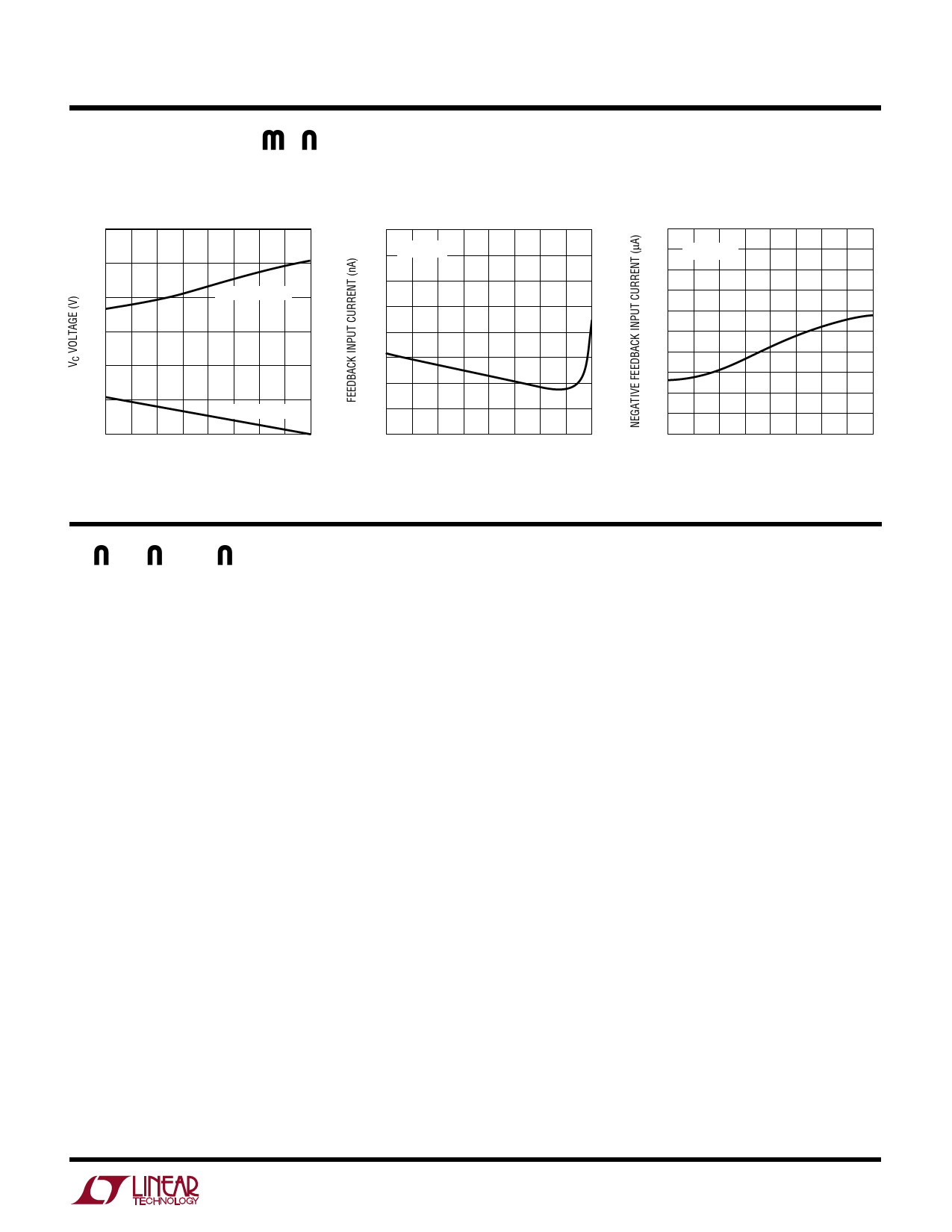
TYPICAL PERFORMANCE CHARACTERISTICS
VC Pin Threshold and High
Clamp Voltage vs Temperature
2.2
2.0
1.8
VC HIGH CLAMP
1.6
1.4
1.2
VC THRESHOLD
1.0
–50 –25 0 25 50 75 100 125 150
TEMPERATURE (°C)
LT1370 • G10
Feedback Input Current
vs Temperature
800
700 VFB =VREF
600
500
400
300
200
100
0
–50 –25
0 25 50 75 100 125 150
TEMPERATURE (°C)
LT1370 • G11
LT1370
Negative Feedback Input Current
vs Temperature
0
VNFB =VNFR
–10
–20
–30
–40
–50
–50 –25
0 25 50 75 100 125 150
TEMPERATURE (°C)
LT1370 • G12
PIN FUNCTIONS
VC: The Compensation pin is used for frequency compen-
sation, current limiting and soft start. It is the output of the
error amplifier and the input of the current comparator.
Loop frequency compensation can be performed with an
RC network connected from the VC pin to ground. See
Applications Information.
FB: The Feedback pin is used for positive output voltage
sensing and oscillator frequency shifting. It is the invert-
ing input to the error amplifier. The noninverting input of
this amplifier is internally tied to a 1.245V reference.
NFB: The Negative Feedback pin is used for negative
output voltage sensing. It is connected to the inverting
input of the negative feedback amplifier through a 100k
source resistor.
S/S: Shutdown and Synchronization Pin. The S/S pin is
logic level compatible. Shutdown is active low and the
shutdown threshold is typically 1.3V. For normal opera-
tion, pull the S/S pin high, tie it to VIN or leave it floating. To
synchronize switching, drive the S/S pin between 600kHz
and 800kHz. See Applications Information.
VIN: Bypass Input Supply Pin with a Low ESR Capacitor,
10µF or More. The regulator goes into undervoltage lock-
out when VIN drops below 2.5V. Undervoltage lockout
stops switching and pulls the VC pin low.
VSW: The Switch pin is the collector of the power switch
and has large currents flowing through it. Keep the traces
to the switching components as short as possible to
minimize radiation and voltage spikes.
GND: Tie all ground pins to a good quality ground plane.
See Applications Information.
5
Share Link: 