236AC1 Просмотр технического описания (PDF) - Linear Technology
Номер в каталоге
Компоненты Описание
производитель
236AC1 Datasheet PDF : 12 Pages
| |||
LT1236
APPLICATIONS INFORMATION
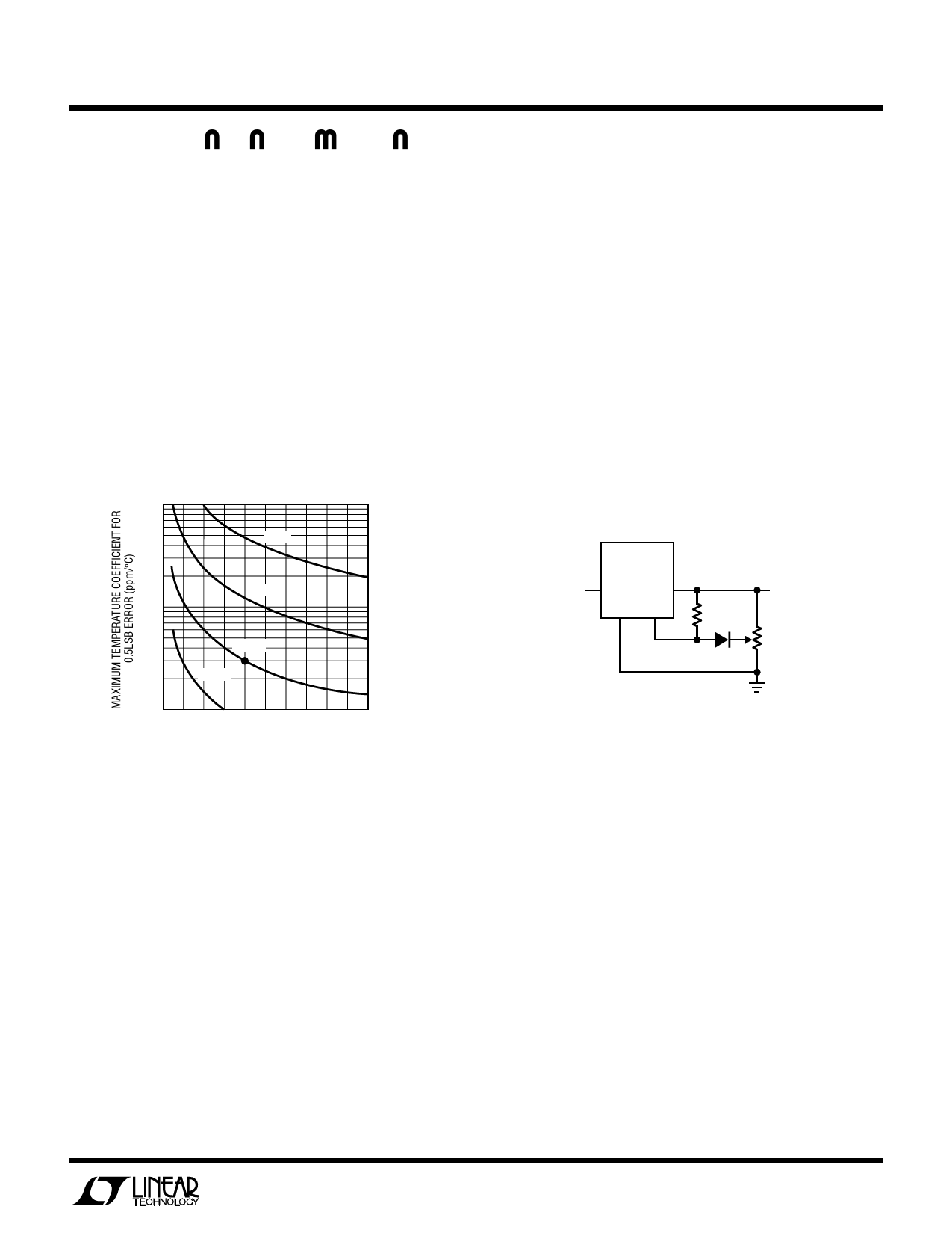
Effect of Reference Drift on System Accuracy
A large portion of the temperature drift error budget in
many systems is the system reference voltage. This graph
indicates the maximum temperature coefficient allowable
if the reference is to contribute no more than 0.5LSB error
to the overall system performance. The example shown is
a 12-bit system designed to operate over a temperature
range from 25°C to 65°C. Assuming the system calibra-
tion is performed at 25°C, the temperature span is 40°C.
It can be seen from the graph that the temperature coeffi-
cient of the reference must be no worse than 3ppm/°C if
it is to contribute less than 0.5LBS error. For this reason,
the LT1236 family has been optimized for low drift.
Maximum Allowable Reference Drift
100
8-BIT
10-BIT
10
12-BIT
14-BIT
in series with a 20kΩ potentiometer will give ±10mV trim
range. Effect on the output TC will be only 1ppm/°C for the
± 5mV trim needed to set the “A” device to 10.000V.
LT1236-5
The LT1236-5 does have an output voltage trim pin, but
the TC of the nominal 4V open circuit voltage at pin 5 is
about –1.7mV/°C. For the voltage trimming not to affect
reference output TC, the external trim voltage must track
the voltage on the trim pin. Input impedance of the trim pin
is about 100kΩ and attenuation to the output is 13:1. The
technique shown below is suggested for trimming the
output of the LT1236-5 while maintaining minimum shift
in output temperature coefficient. The R1/R2 ratio is
chosen to minimize interaction of trimming and TC shifts,
so the exact values shown should be used.
LT1236-5
IN
OUT
GND TRIM
R1
27k
1N4148
VOUT
R2
50k
1.0
10 20 30 40 50 60 70 80 90 100
TEMPERATURE SPAN (°C)
LT1236 AI01
Trimming Output Voltage
The LT1236-10 has a trim pin for adjusting output voltage.
The impedance of the trim pin is about 12kΩ with a
nominal open circuit voltage of 5V. It is designed to be
driven from a source impedance of 3kΩ or less to mini-
mize changes in the LT1236 TC with output trimming.
Attenuation between the trim pin and the output is 70:1.
This allows ±70mV trim range when the trim pin is tied to
the wiper of a potentiometer connected between the
output and ground. A 10kΩ potentiometer is recom-
mended, preferably a 20 turn cermet type with stable
characteristics over time and temperature.
The LT1236-10 “A” version is pre-trimmed to ±5mV and
therefore can utilize a restricted trim range. A 75k resistor
LT1236 AI02
Capacitive Loading and Transient Response
The LT1236 is stable with all capacitive loads, but for
optimum settling with load transients, output capacitance
should be under 1000pF. The output stage of the reference
is class AB with a fairly low idling current. This makes
transient response worse-case at light load currents.
Because of internal current drain on the output, actual
worst-case occurs at ILOAD = 0 on LT1236-5 and ILOAD =
1.4mA (sinking) on LT1236-10. Significantly better load
transient response is obtained by moving slightly away
from these points. See Load Transient Response curves
for details. In general, best transient response is obtained
when the output is sourcing current. In critical applica-
tions, a 10µF solid tantalum capacitor with several ohms
in series provides optimum output bypass.
7
Share Link: 