LT1032CN(RevC) Просмотр технического описания (PDF) - Linear Technology
Номер в каталоге
Компоненты Описание
производитель
LT1032CN Datasheet PDF : 8 Pages
| |||
LT1032
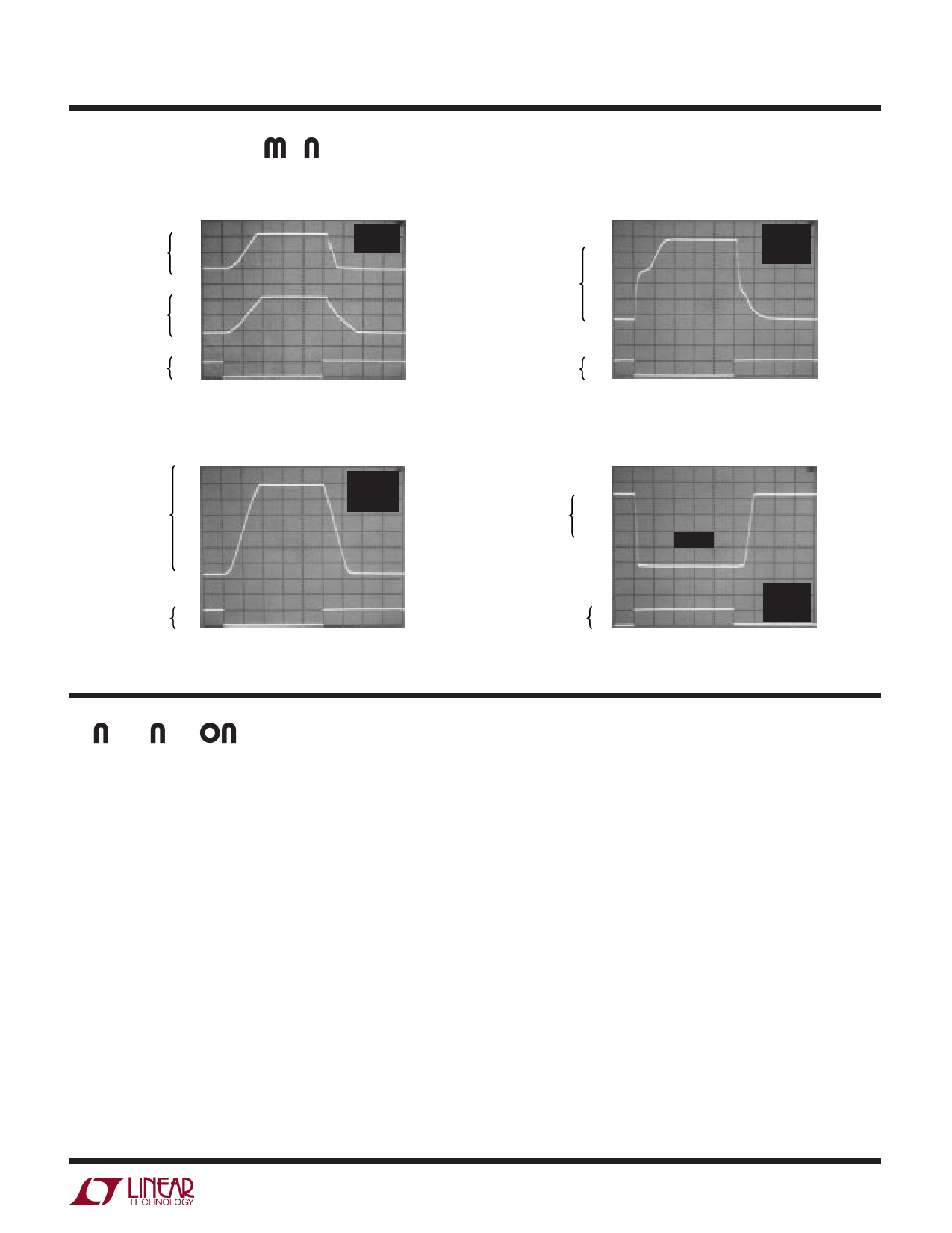
PI FU CTI S
VEE (J, N & S: Pin 1): Minus Supply. Operates –2V to –15V.
(J & N: Pins 2, 5, 9, 12/S: Pins 2, 5, 11, 14): Logic
Input. Operates properly on TTL or CMOS levels. Output
valid form (V– + 2V) ≤ VIN ≤ 15V. Connect to ground
when not used.
(J & N: Pins 3, 6, 8, 11/S: Pins 3, 6, 10, 13): Output. Line
drive output.
ON/OFF (J, N & S: Pin 4): Shuts down entire circuit.
Cannot be left open. For “normally on” operation, connect
to V +.
GND (J, N & S: Pin 7): Ground. Ground must be more
positive than V–.
Response Control (J & N: Pin 10/S: Pin 12): Allows
limited change of slew rate. Leave open when not used.
Strobe (J & N: Pin 13/ S: Pin 15): Forces all outputs low.
Drive with 3V.
VCC (J & N:Pin 14/S: Pin 15): Positive Supply. Operates 5V
to 15V.
APPLICATI S I FOR ATIO
Application Hints
The LT1032 is exceptionally easy to use when compared to
older drivers. Operating supply voltage can be as low as ±3V
or as high as ±15V. Input levels are referred to ground.
The logic inputs are internally set at TTL levels. Outputs are
valid for input voltages from 1V above V – to 25V. Driving the
logic inputs to V – turns off the output stage. The ON/OFF
control completely turns off all supply current of the LT1032.
The levels required to drive the device on or off are set by
internal emitter-based voltages. Since the current into the
ON/OFF pin is so low, TTL or CMOS drivers have no problem
controlling the device.
The strobe pin is not fully logic compatible. The impedance
of the strobe pin is about 2kΩ to ground. Driving the strobe
pin positive forces the output stages low–even if the device
is shut off. Under worst case conditions, 3V minimum at
2mA are needed driving the strobe pin to insure strobing.
The response pin can be used to make some adjustment in
slew rate. A resistor can be connected between the re-
sponse pin and the power supplies to drive 50µA to 100µA
into the pin. The response pin is a low impedance point
operating at about 0.75V above ground. For supply voltage
up to ±6V, current is turned off when the device is turned off.
For higher supply voltages, a Zener should be connected in
series with the resistor to limit the voltage applied to the
response pin to 6V. Also, for temperatures above 100°C,
using the response pin is not recommended. The leakage
current into the response pin at high temperatures is
excessive.
Outputs are well protected against shorts or externally
applied voltage. Tested limits are ±30V, but the device can
withstand external voltages up to breakdown of the transis-
tors (typically about 50V). The LT1032 is usually immune to
ESD up to 2500V on the outputs with no damage.
TYPICAL APPLICATI S
Protecting Against More Than ±30V Output Overload
V+
INPUT
1/4 LT1032
100Ω TO
1000Ω
TO LINE
INPUT
1/4 LT1032
V–
LT1032 • TA03a
TO LINE
30V ZENERS
LT1032 • TA03b
5
Share Link: 