JLM2904WH-CD1 Просмотр технического описания (PDF) - STMicroelectronics
Номер в каталоге
Компоненты Описание
производитель
JLM2904WH-CD1 Datasheet PDF : 12 Pages
| |||
LM2904WH
Absolute maximum ratings and operating conditions
2
Absolute maximum ratings and operating conditions
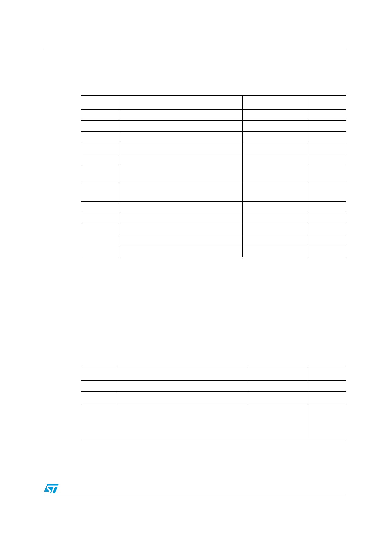
Table 1. Absolute maximum ratings
Symbol
Parameter
Value
Unit
VCC+
Vid
Vin
Supply voltage
Differential input voltage
Input voltage
Output short-circuit to ground(1)
+32
V
-0.3 to VCC+0.3
V
-0.3 to VCC+0.3
V
40
mA
Tj
Rthja
Rthjc
Iin
Tstg
ESD
Maximum junction temperature
Thermal resistance junction to ambient (2)
SO-8
Thermal resistance junction to case (2)
SO-8
Input current (3)
Storage temperature range
HBM: human body model(4)
MM: machine model(5)
CDM: charged device model(6)
150
125
40
5
-65 to +150
2
200
1.5
°C
°C/W
°C/W
mA
°C
kV
V
kV
1. Short-circuits from the output to VCC can cause excessive heating if VCC+ > 15 V. The maximum output
current is approximately 40 mA, independent of the magnitude of VCC. Destructive dissipation can result
from simultaneous short-circuits on all amplifiers.
2. Short-circuits can cause excessive heating and destructive dissipation. Values are typical.
3. This input current only exists when the voltage values applied on the inputs is beyond the supply voltage
line limits. This is not destructive if the current does not exceed 5 mA as indicated, and normal output is
restored for input voltages above -0.3V.
4. Human body model: A 100pF capacitor is charged to the specified voltage, then discharged through a
1.5kΩ resistor between two pins of the device. This is done for all couples of connected pin combinations
while the other pins are floating.
5. Machine model: A 200pF capacitor is charged to the specified voltage, then discharged directly between
two pins of the device with no external series resistor (internal resistor < 5Ω). This is done for all couples of
connected pin combinations while the other pins are floating.
6. Charged device model: all pins and the package are charged together to the specified voltage and then
discharged directly to the ground through only one pin. This is done for all pins.
Table 2. Operating conditions
Symbol
Parameter
Value
Unit
VCC+
Supply voltage
3 to 30
V
Toper Operating free-air temperature range
-40 to +150
°C
Vicm
Input common mode voltage range
(VCC+=+30V)(1)
Tamb = 25°C
Tmin ≤ Tamb ≤ Tmax
0 to VCC+ -1.5
V
0 to VCC+ -2
1. The input common-mode voltage of either input signal voltage should not be allowed to go negative by
more than 0.3 V. The upper end of the common-mode voltage range is VCC+ –1.5 V, but either or both
inputs can go to +32 V without damage.
3/12
Share Link: 