LC822152 Просмотр технического описания (PDF) - SANYO -> Panasonic
Номер в каталоге
Компоненты Описание
производитель
LC822152 Datasheet PDF : 11 Pages
| |||
Continued from preceding page.
• I2C Interface
• Scaling function
• JPEG codec
• Thumbnail
• Clock system
• Package
• Process
• Power source voltage
LC822152
Built-in I2C master for CCD/CMOS module control. Without paying attention to the
I2C from the CPU, it is accessible to the CCD/CMOS module as well as the normal
register (write/read).
CCD output is a VGA size (640×480). The output is reduced/cropped to meet the LCD
display range with a scaler. Low-pass filter and enhancer are equipped.
The YUV422/YUV420 image data is compressed into JPEG code, and the JPEG code
data is expanded to the YUV422/YUV420 image data.
It performs thinning out, scaling down and cropping the LCD output images to an
image size of maximum 40×40.
LSI includes PLL and it multiplies the clock input from outside to make a main clock.
It divides this multiplied frequency to output to CCD/CMOS module as the clock.
FBGA96K
0.18µm E/A
Internal 1.8V±0.18V, I/O 3.0V±0.3V
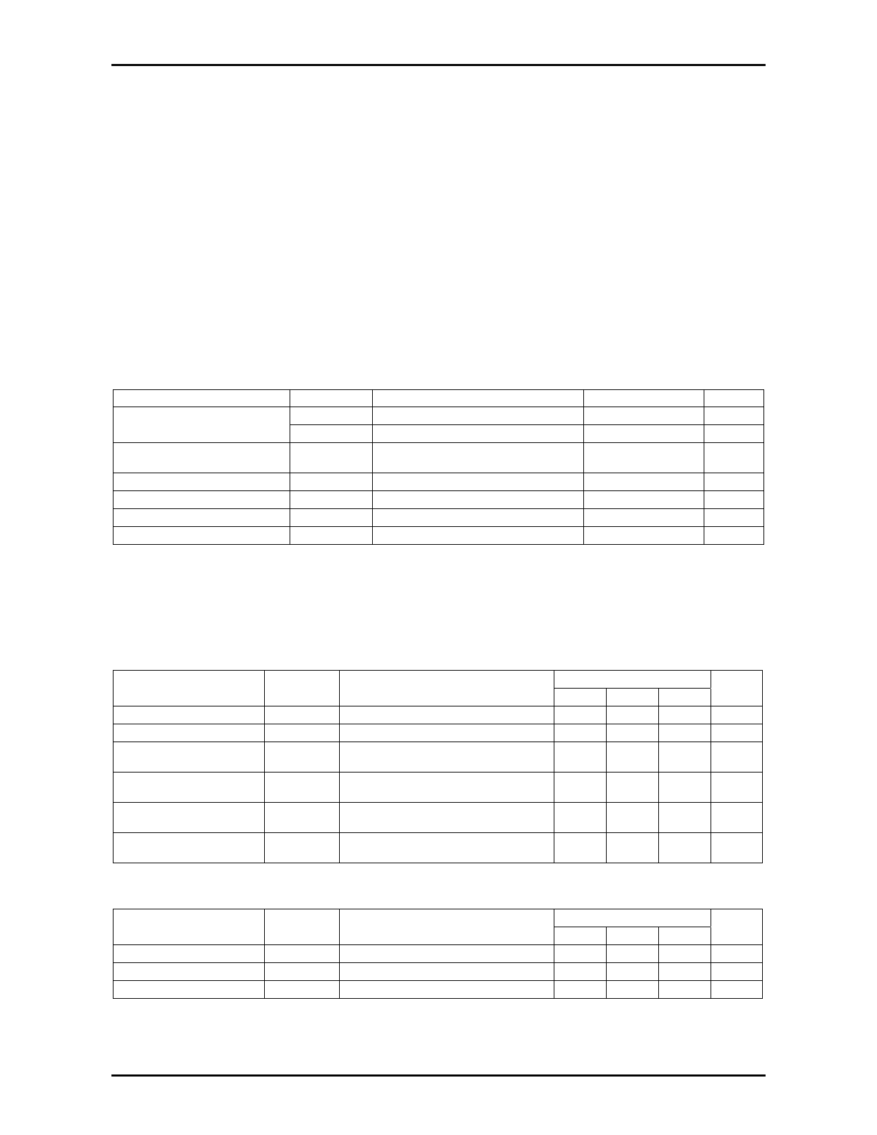
Specifications
Absolute Maximum Ratings at VSS = 0V
Parameter
Symbol
Conditions
Ratings
Unit
Source Voltage
VDD30 max
-0.3 to 3.3
V
VDD18 max
-0.3 to 1.98
V
Input/Output Voltage
VI, VO
-0.3 to *VDD3 max
V
*+0.3 (max 3.3V)
Input/Output Current
II, IO
*1
±20
mA
Allowable Power Dissipation
Pd max
Ta≤70°C *2
650
mW
Operating Temperature
Topr
-30 to +70
°C
Storage Temperature
Tstg
-55 to +125
°C
*1 : Absolute maximum rating per input/output reference cell
*2 : This value is assured when the conditions for substrate mounting are as follows.
In other conditions, the assured value will be changed accordingly. (Conditions for substrate mounting)
Substrate size : FR4 (50mm×108mm×1.27mm)
Cu trace rate : 250%
Allowable Operating Range at Ta = -30 to +70°C, VSS = 0V
Parameter
Symbol
Power Source Voltage (I/O unit)
Input Voltage Range (I/O unit)
Source Voltage
(Internal logic unit)
Input Voltage Range
(Internal logic unit)
Power Source Voltage
(Analog part)
Input Voltage Range
(Analog part)
VDD30
VIN30
VDD18
VIN18
AVDD
AVIN
Conditions
Ratings
Unit
min
typ
max
2.7
3.0
3.3
V
0
VDD30
V
1.62
1.8
1.98
V
0
VDD18
V
1.62
1.8
1.98
V
0
AVDD
V
Input/Output Pin Capacitance at Ta = 25°C, VDD18 = VDD33 = VIN18 = VIN30 = 0V
Parameter
Input Pin
Output Pin
Input/Output Pin
Symbol
CIN
COUT
CI/O
f = 1MHz
f = 1MHz
f = 1MHz
Conditions
Ratings
Unit
min
typ
max
10
pF
10
pF
10
pF
No.8075-2/11
Share Link: 