LC74798 Просмотр технического описания (PDF) - SANYO -> Panasonic
Номер в каталоге
Компоненты Описание
производитель
LC74798 Datasheet PDF : 32 Pages
| |||
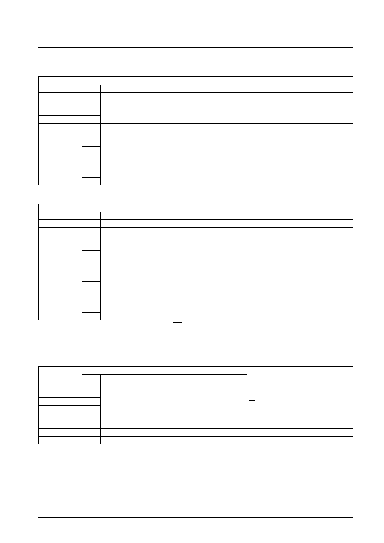
LC74798, 74798M
COMMAND0 (Display memory write address setup command)
• First byte
DA
0 to 7
7
6
5
4
Register
—
—
—
—
3
V3
2
V2
1
V1
0
V0
State
1
0
0
0
0
1
0
1
0
1
0
1
Contents
Function
Command 0 identification code.
Sets the display memory write address.
Display memory line address (0 to B hexadecimal)
• Second byte
DA
0 to 7
Register
State
Contents
Function
7
—
0 Second byte identification bit
6
—
0
5
—
0
0
4
H4
1
0
3
H3
1
2
H2
0
Display memory column address (0 to 17 hexadecimal)
1
0
1
H1
1
0
0
H0
1
Note: All registers are set to 0 when the LC74798/M is reset by the RST pin.
COMMAND1 (Display character data write setup command)
• First byte
DA
0 to 7
7
6
5
4
3
2
1
0
Register
—
—
—
—
—
—
—
—
State
1
0
0
1
0
0
0
0
Contents
Function
Command 1 identification code.
Sets up display character data write mode.
Notes
Notes
Notes
When this command is input, the LC74798/M locks
in the display character data write mode until the
CS pin goes high
No. 5833-9/32
Share Link: 