LC74798 Просмотр технического описания (PDF) - SANYO -> Panasonic
Номер в каталоге
Компоненты Описание
производитель
LC74798 Datasheet PDF : 32 Pages
| |||
Continued from preceding page.
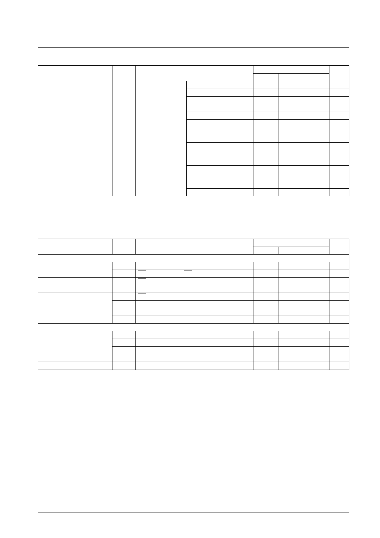
LC74798, 74798M
Parameter
Symbol
Conditions
Background color low level
VRSL
(1)
CVOUT : VDD1 = 5.0 V, (2)
VDD2 = 5.0 V (3)
Background color high level
VRSH
(1)
CVOUT : VDD1 = 5.0 V, (2)
VDD2 = 5.0 V (3)
Frame level 0
VBK0
(1)
CVOUT : VDD1 = 5.0 V, (2)
VDD2 = 5.0 V (3)
Frame level 1
VBK1
(1)
CVOUT : VDD1 = 5.0 V, (2)
VDD2 = 5.0 V (3)
Character level
VCHA
(1)
CVOUT : VDD1 = 5.0 V, (2)
VDD2 = 5.0 V (3)
Notes: (1): When the sync level = 0.8 V
(2): When the sync level = 1.0 V
(3): When the sync level = 1.4 V
The values in parentheses for the background high and low levels are for blue background mode.
Timing Characteristics at Ta = –30 to +70°C, VDD1 = 5 ±0.5 V
Parameter
Symbol
Conditions
OSD write (See figure 1.)
Minimum input pulse width
tW (SCLK) SCLK1
tW (CS1) CS1 (The period when CS1 is high)
Data setup time
tSU (CS1) CS1
tSU (SIN) SIN1
Data hold time
th (CS1)
th (SIN)
CS1
SIN1
One word write time
tword
twt
The 8-bit data write time
The RAM data write time
PDC/VPS write (For the n-channel open-drain output circuit type. See figure 2)
Minimum input pulse width
Setup time
Output delay time
tCKCY
tCKL
tCKH
tICK
tCKO
SCLK2
SCLK2
SCLK2
SCLK2
DOUT
Note: The OSD timing applies when the CMOS output circuit type is used.
Ratings
Unit
min
typ
max
1.23 (1.16)
V
1.43 (1.36)
V
1.83 (1.76)
V
2.37 (2.01)
V
2.57 (2.21)
V
2.97 (2.61)
V
1.50
V
1.70
V
2.10
V
2.08
V
2.28
V
2.68
V
2.65
V
2.85
V
3.25
V
Ratings
Unit
min
typ
max
200
ns
1
µs
200
ns
200
ns
2
µs
200
ns
4.2
µs
1
µs
2
µs
1
µs
1
µs
10
µs
0.5
µs
No. 5833-5/32
Share Link: 