LC74772V Просмотр технического описания (PDF) - SANYO -> Panasonic
Номер в каталоге
Компоненты Описание
производитель
LC74772V Datasheet PDF : 17 Pages
| |||
LC74772V
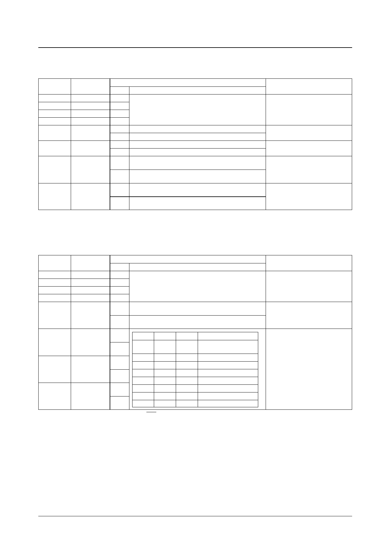
} COMMAND 5 (Display control: on/off settings for each output system)
First byte
DA0 to DA7
7
6
5
4
3
2
1
Register name
—
—
—
—
DSP4
DSP3
DSP2
State
0
1
0
1
0
1
0
1
Register content
Function
Command 5 identification code
System 4 output off
System 4 output on
System 3 output off
System 3 output on
0 System 2 output off
1 System 2 output on
0 System 1 (RGB) output off
0
DSP1
1 System 1 (RGB) output on
Note
Pin 10 (BLK4) and pin 11 (CHA4) output
control
Pin 14 (BLK3) and pin 15 (CHA3) output
control
Pin 16 (BLK2) and pin 17 (CHA2) output
control
Invalid in RGB output mode.
Pin 18 (BLK1) and pin 19 (CHA1) output
control
Functions as the RGB output control in
RGB output mode.
~ COMMAND 6 (Output control: systems 3 and 4 output control settings)
First byte
DA0 to DA7
7
6
5
4
3
Register name
—
—
—
—
DSPF
SL34
State
0
1
1
0
0
1
Register content
Function
Command 6 identification code
Sets the system 3 output conditions according to the command
described below.
Sets the system 4 output conditions according to the command
described below.
0
DSPRSG DSPGSG DSPBSG
Output selection
2
DSP
RSG
Signals other than R, G,
1
0
0
0
B are output.
0
0
1
B is output.
1
DSP
GSG
0
0
1
0
G is output.
0
1
1
G and B are output.
1
1
0
0
R is output.
0
1
0
1
R and B are output.
0
DSP
BSG
1
1
0
R and G are output.
1
1
1
1
All of R, G, B are output.
Note: This register is set to 0 on a reset (either by the RST pin or by a command reset).
Note
Only system 4 is valid in 4-system
output mode. System 4 cannot be set
when the general-purpose output port
usage is specified.
Note: The following registers are set to
1 during a reset.
DSPRSG
DSPGSG
DSPBSG
As a result, the “All of R, G, B are
output” state is selected during a
reset.
No. 5159-10/17
Share Link: 