LC651154F Просмотр технического описания (PDF) - SANYO -> Panasonic
Номер в каталоге
Компоненты Описание
производитель
LC651154F Datasheet PDF : 39 Pages
| |||
LC651154N, 651154F, 651154L, 651152N, 651152F, 651152L
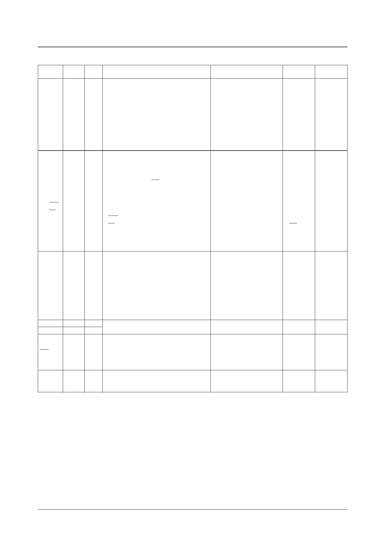
Continued from preceding page.
Symbol
Number
of pins
PE0-PE1/
2
WDR
I/O
Function
Option
• I/O port E0 to E1
Input in 4-bit units (IP instruction)
(1) Open-drain output
Output in 4-bit units (OP instruction)
(2) Pull-up resistor
Set and reset in 1-bit units (SPB and RPB
• Options (1) and (2) can be
I/O
instructions)
specified in bit units
Testing in 1-bit units (BP and BNP instructions)
(3) Normal port PE1
• PE0 also has a continuous pulse (64·Tcyc) output
function.
• PE1 becomes the watchdog reset pin WDR when
selected for such as an option.
(4) Watchdog reset WDR
• Either options (3) and (4)
may be specified.
PF0/SI
PF1/SO
4
PF2/SCK
PF3/INT
• I/O port F0 to F3
The port functions and options are identical to
those of PE0 to PE1 (See note.)
• PF0 to PF3 have shared functions as the serial
interface pins and the INT input.
The function can be selected under program
control.
I/O
SI ... Serial input pin
Identical to those for PA0 to PA3
SO ... Serial output pin
SCK ... Input and output of the serial clock signal
INT ... Interrupt request input
The serial I/O function can be switched between 4-
bit and 8-bit transfers under program control.
Note: There is no continuous pulse output function.
PG0-PG3/
4
AD4-AD7
AV+
1
AV–
1
RES
1
I/O
—
—
Input
• I/O port G0 to G3
The port functions and options are identical to
those of PE0 to PE1 (See note.)
Note: There is no continuous pulse output function.
• All four pins have shared functions.
PG0/AD4 - A/D converter input AD4
Identical to those for PA0 to PA3
PG1/AD5 - A/D converter input AD5
PG2/AD6 - A/D converter input AD6
PG3/AD7 - A/D converter input AD7
A/D converter reference voltage input
—
• System reset input
• Applications must provide an external capacitor for
the power-on reset.
—
• Apply a low level to this pin for 4 clock cycles to
effect and reset start.
TEST
• IC test pin
1
Input This pin must be connected to VSS during normal —
operation.
At reset
Handling when
unused
High-level
output (The
output n-
channel
transistors in
the off state.)
Identical to
those for PA0
to PA3
Identical to
those for PA0
to PA3
The serial port Identical to
functions are those for PA0
disabled.
to PA3
The interrupt
source is set
to INT.
Identical to Identical to
those for PA0 those for PA0
to PA3
to PA3
Connect to
—
VSS.
—
—
This pin must
—
be connected
to VSS.
No. 6278-8/39
Share Link: 