L6911C Просмотр технического описания (PDF) - STMicroelectronics
Номер в каталоге
Компоненты Описание
производитель
L6911C Datasheet PDF : 20 Pages
| |||
L6911C
overcurrent protection this relationship must be satisfied:
IP
≥
IOUTMAX
+
-∆---l
2
=
IPEAK
Where ∆I is the inductance ripple current and IOUTMAX is the maximum output current.
In case of output short circuit the soft start capacitor is discharged with constant current (10µA typ.) and when
the SS pin reaches 0.5V the soft start phase is restarted. During the soft start the over-current protection is al-
ways active and if such kind of event occurs, the device turns off both mosfets, and the SS capacitor is dis-
charged again (after reaching the upper threshold of about 4V). The system is now working in HICCUP mode,
as shown in figure 5a. After removing the cause of the over-current, the device restart working normally without
power supplies turn off and on.
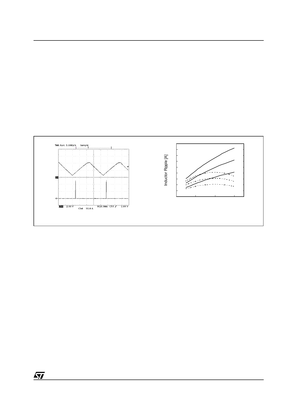
Figure 5.
a: Hiccup Mode
9
8
7
6
5
4
3
2
1
0
0.5
L=1.5µH, Vin=12V
L=2µH,
Vin=12V
L=3µH,
Vin=12V
L=1.5µH,
Vin=5V
L=2µH,
Vin=5V
L=3µH, Vin=5V
1.5
2.5
3.5
Output Voltage [V]
b: Inductor Ripple Current vs. Vout
Inductor design
The inductance value is defined by a compromise between the transient response time, the efficiency, the cost
and the size. The inductor has to be calculated to sustain the output and the input voltage variation to maintain
the ripple current ∆IL between 20% and 30% of the maximum output current. The inductance value can be cal-
culated with this relationship:
L
=
-V----I-N-f-S---–--⋅---V∆----OI--L--U----T--
⋅
V-----O----U----T-
VIN
Where fSW is the switching frequency, VIN is the input voltage and VOUT is the output voltage. Figure 5b shows
the ripple current vs. the output voltage for different values of the inductor, with VIN = 5V and VIN = 12V.
Increasing the value of the inductance reduces the ripple current but, at the same time, reduces the converter
response time to a load transient. If the compensation network is well designed, the device is able to open or
close the duty cycle up to 100% or down to 0%. The response time is now the time required by the inductor to
change its current from initial to final value. Since the inductor has not finished its charging time, the output cur-
rent is supplied by the output capacitors. Minimizing the response time can minimize the output capacitance
required.
The response time to a load transient is different for the application or the removal of the load: if during the ap-
plication of the load the inductor is charged by a voltage equal to the difference between the input and the output
voltage, during the removal it is discharged only by the output voltage. The following expressions give approx-
imate response time for ∆I load transient in case of enough fast compensation network response:
9/20
Share Link: 