L6668 Просмотр технического описания (PDF) - STMicroelectronics
Номер в каталоге
Компоненты Описание
производитель
L6668 Datasheet PDF : 23 Pages
| |||
L6668
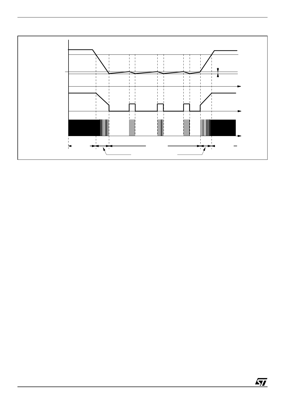
Figure 40. Load-dependent operating modes: timing diagram
COMP
3.0V
V(SKIPADJ)
fosc
50 mV
hyster.
t
t
OUT
Fix. Freq.
Mode
Burst-mode
Frequency Foldback Mode
t
Fix. Freq.
Mode
The operating range of the voltage V(SKIPADJ) is practically limited upwards by the onset of audible
noise: typically, with a voltage above 2-2.1V some noise can be heard under some line/load conditions. If,
instead, V(SKIPADJ) is set below the low saturation value of the PWM control voltage (1.4V typ.) burst-
mode operation will never take place. Always bias the pin at some voltage, a floating pin will result in
anomalous behavior. The SKIPADJ pin doubles its function: if the voltage is pulled below 0.8V the IC is
disabled completely, except for the externally available reference voltage VREF, and its quiescent con-
sumption reduced. The soft-start capacitor is discharged so that, when the voltage on the SKIPADJ pin is
pulled above 0.8V, the chip is soft-started just like exiting from UVLO. This function is useful for some kind
of remote ON/OFF control. The comparator referenced to 0.8V does not have hysteresis; hence make
sure that the voltage on the pin does not linger on the threshold to prevent uncertain behavior.
4.4 PWM control Block
The device is specific for secondary feedback. Typically, there is a TL431 at the secondary side and an
optocoupler that transfers output voltage information to the PWM control at the primary side, crossing the
isolation barrier. The PWM control input (pin #10, COMP) is driven directly by the phototransistor's col-
lector (the emitter is grounded to GND) to modulate the duty cycle.
4.5 Current Comparator, PWM Latch and Hiccup-mode OCP
The current comparator senses the voltage across the current sense resistor (Rs) on pin 12 (ISEN) and,
by comparing it with the programming signal derived form the control voltage on pin 10 (COMP), deter-
mines the exact time when the external MOSFET is to be switched off. The PWM latch avoids spurious
switching of the MOSFET, which might result from the noise generated ("double-pulse suppression").
16/23
Share Link: 