L6181A Просмотр технического описания (PDF) - STMicroelectronics
Номер в каталоге
Компоненты Описание
производитель
L6181A Datasheet PDF : 10 Pages
| |||
L6180 - L6181
ELECTRICAL CHARACTERISTICS (VCC = 5V ±5%; VCM = -7 to 7V; Tamb = 0 to 70°C;
VSS = -9 to 13.5V; VDD = 9 to 13.5V; unless otherwise specified.)
Symbol
fR
Parameter
Frequency Rejected
(No Receiver Output)
Test Condition
VIN = 2Vpp;
(see fig. 8 and note 7)
Min.
Typ.
5
Max.
Unit
MHz
Note:
1) The algebric convention, where the less positive (more negative) is designed the minimum
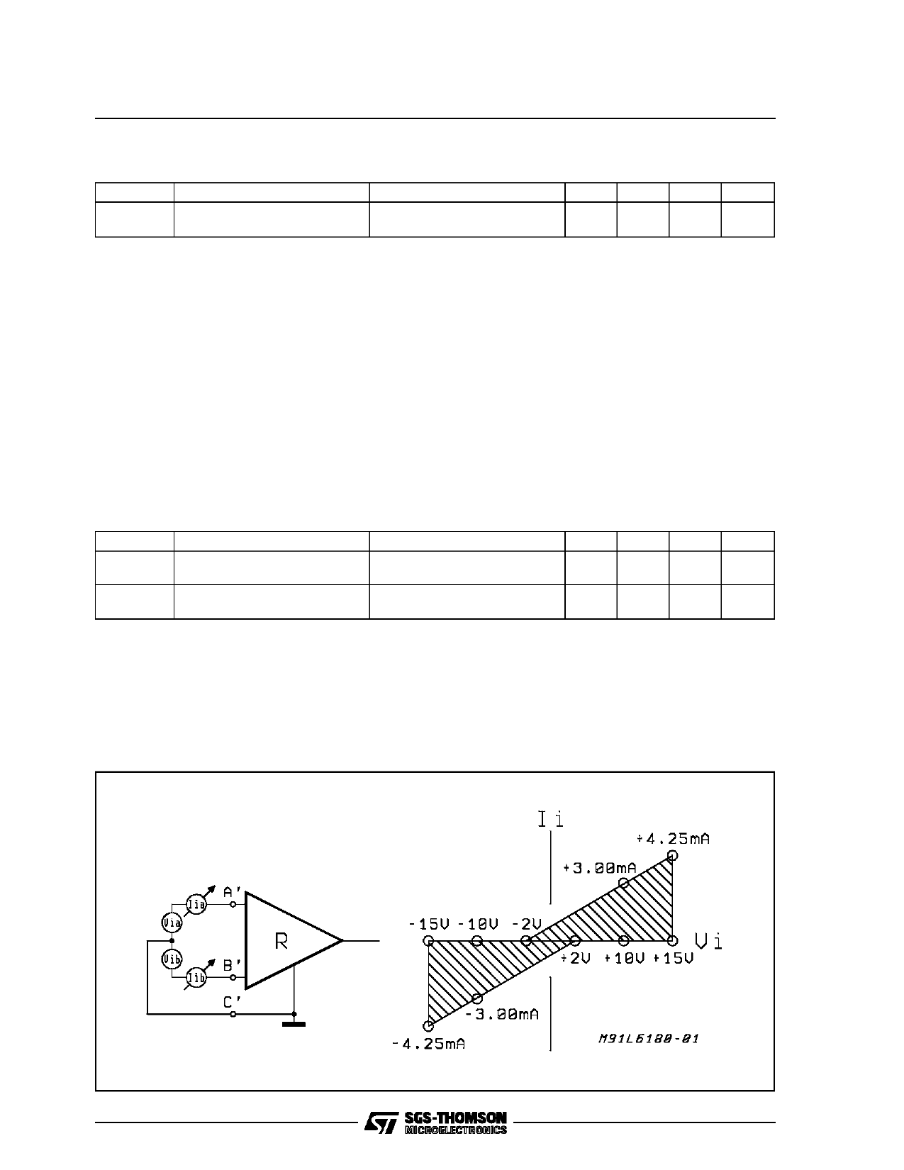
2) With the voltage VIA or (VIB) ranging between ±15V, while VIB or (VIA) is open or grounded, the resultant input current IIA or (IIB) shall remain
within the shaded region shown in the graph in Fig.1.
3) Either Point B’ or Point A’ is grounded in Figure 1
4) VICC measured from grounded to (+) input with (-) input grounded
VICC measured from grounded to (+) input with (-) input grounded
5) Not more than one output should be shorted at a time and for less than 1 seond
6) The sum of the product of the maximum supply currents and voltages cannot exceed themaximum power dissipation
7) A: The conditions for the inpit switching from VIOCL to VIOCH mode is: Vid in start bit ”spacing condition”for less than TpVioch (5ms).
B: The conditions for the input switching from VIOCH to VIOCL mode is: Vid > WW2 for greater than TpVIOCL (200ms)
8) An example of a frequency response plot meeting the rejection/acceptance requirements is provided in figure 8.
LINE TRANSIENT IMMUNITY (Considering the following cases; powered ON, Powered OFF-LOW im-
pedance power supply and powered OFF-HIGH impedance supply)
Symbol
ESD
Static
Parameter
EOS
Stress
Test Condition
tested per MIL-STD-883
(see note 9)
transient pulse both polarities
for 100µs (see note 9 and Fig. 2)
Min.
2
50
Typ.
Max.
Note:
9) All pins are required to withstand this parameters.
10) Input pins are required to withstand fig.2 without any degradation to the circuit.
11) The balance test requirement can be met by use of a current limit circuit which reduces the input bias current Iib (see figure 7)
for input voltages below a threshold voltage given by (Iib x 1K) - 400mV.
Unit
KV
V
Figure 1: Input Current Voltage Mesurements
4/10
Share Link: 